# A B C D E F G H I J K L M N O P Q R S T U V W X Y Z

AD8311 Analog Devices Data Handbook/Manual

Summary

This RF detector/controller is a complete, high-sensitivity subsystem designed for precise power monitoring and control in mobile and wireless devices. It delivers an accurate, temperature-stable voltage output ideal for directly controlling radio frequency power amplifiers across a wide spectrum (0.1 to 2.5 GHz). The accompanying documentation provides comprehensive coverage, detailing theory of operation, calibration methods, pin configuration, and connection guidelines necessary for system integration by communication engineers building advanced cellular handsets.
📄 Preview PAGE OF 24

Page 1 Text Content

50 d B GSM PA Controller

AD8311

Its high sensitivity allows control at low signal levels, thus

FEATURES

reducing the amount of power that needs to be coupled to the

Complete RF detector/controller function

detector. For convenience, the signal is internally ac-coupled.

>50 d B range at 0.9 GHz (−48 d Bm to +3 d Bm re 50 Ω)

This high-pass coupling, with a corner at approximately

Accurate scaling from 0.1 GHz to 2.5 GHz

0.016 GHz, determines the lowest operating frequency. Thus,

Temperature-stable linear-in-d B response

the source can be dc-grounded.

Log slope of 23 m V/d B, intercept at −60 d Bm at 0.9 GHz True integration function in control loop The AD8311 provides a voltage output, VAPC, which has the Low power: 20 m W at 2.7 V voltage range and current drive to directly connect to the gain

control pin of most handset power amplifiers. VAPC can swing from 300 m V above ground to within 200 m V below the supply

APPLICATIONS

voltage. Load currents of up to 6 m A can be supported.

Single, dual, and triple band mobile handset (GSM, DCS, EDGE)

The setpoint control input is applied to pin VSET and has an

Transmitter power control

operating range of 0.25 V to 1.4 V. The associated circuit determines the slope and intercept of the linear-in-d B GENERAL DESCRIPTION measurement system; these are nominally 23.6 m V/d B and −59.7 d Bm at 0.9 GHz. Further simplifying the application of

The AD8311 is a complete low cost subsystem for the precise

the AD8311, the input resistance of the setpoint interface is over

control of RF power amplifiers operating in the frequency range

35 MΩ, and the bias current is typically 0.26 µA.

0.1 GHz to 2.5 GHz and over a typical dynamic range of 50 d B. It is intended for use in cellular handsets and other battery- The AD8311 is available in a 6-ball wafer-level chip scale operated wireless devices. The log amp technique provides a package (WLCSP), 1.0 mm × 1.5 mm, and consumes 7.6 m A much wider measurement range and better accuracy than www.BDTIC.com/ADI from a 2.7 V to 5.5 V supply. controllers using diode detectors. In particular, its temperature stability is excellent over a specified range of −40°C to +85°C.

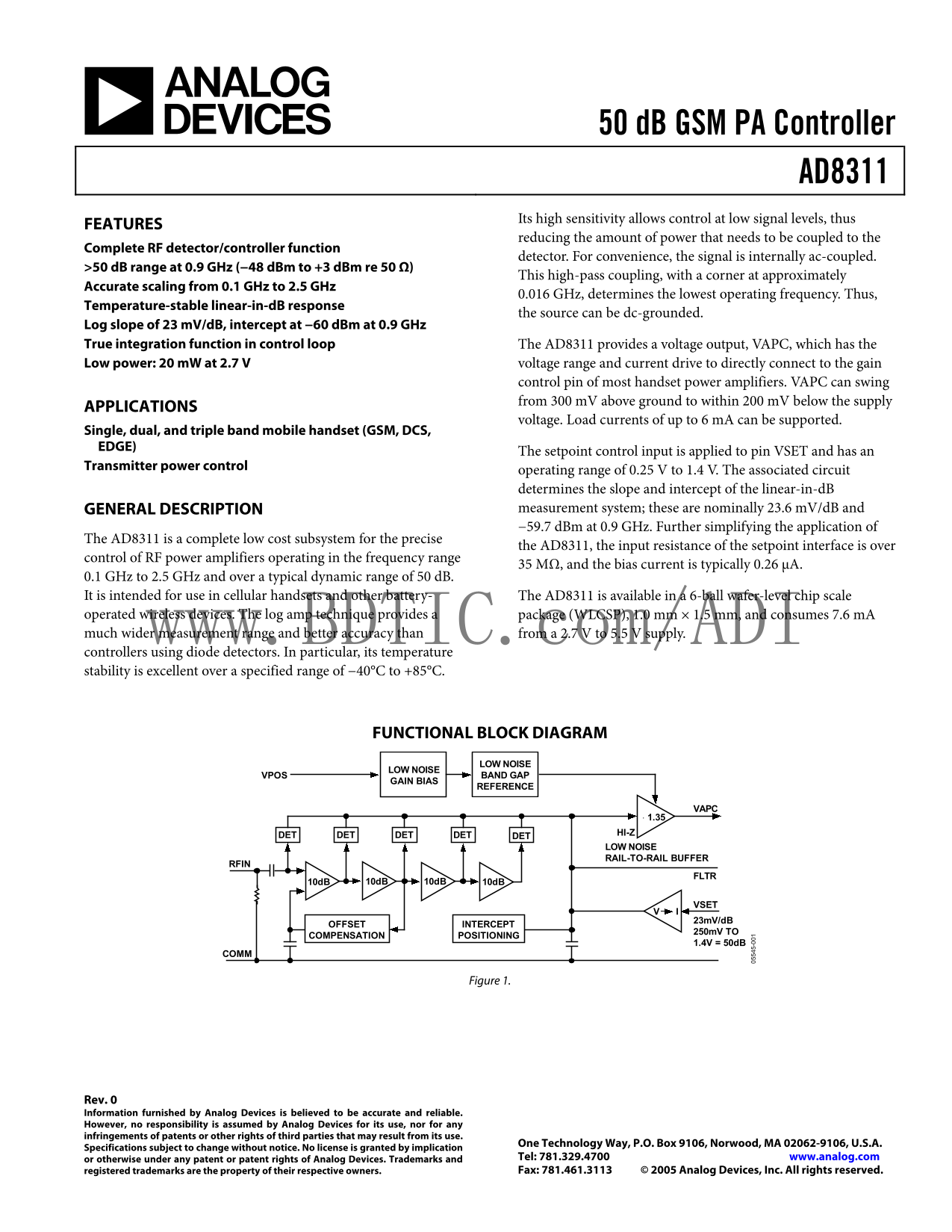
FUNCTIONAL BLOCK DIAGRAM

LOW NOISE

LOW NOISE

VPOS BAND GAP

GAIN BIAS

REFERENCE

1.35 HI-Z

DETDETDETDETDET

LOW NOISE RAIL-TO-RAIL BUFFER

OFFSET INTERCEPT

250m V TO

COMPENSATION POSITIONING

Figure 1.

Rev. 0 Information furnished by Analog Devices is believed to be accurate and reliable. However, no responsibility is assumed by Analog Devices for its use, nor for any infringements of patents or other rights of third parties that may result from its use.

One Technology Way, P.O. Box 9106, Norwood, MA 02062-9106, U.S.A.

Specifications subject to change without notice. No license is granted by implication

or otherwise under any patent or patent rights of Analog Devices. Trademarks and Tel: 781.329.4700 www.analog.com registered trademarks are the property of their respective owners. Fax: 781.461.3113 © 2005 Analog Devices, Inc. All rights reserved.

Page Summary Contents For AD8311 Analog Devices Data Handbook/Manual

Page 1 50 d B GSM PA Controller AD8311 Its high sensitivity allows control at low signal levels, thus FEATURES reducing the amount of power that needs to be coupled to the Complete RF detector/controller fun...
Page 2 AD8311 TABLE OF CONTENTS Specifications..................................................................................... Mobile Handset Power Control Example Absolute Maximum Ratings.................
Page 3 AD8311 SPECIFICATIONS VPOS = 2.7 V, Frequency = 0.1 GHz, TA = 25°C, 52.3 Ω termination on RFIN, light condition = 600 lux, unless otherwise noted. Table 1. Parameter Conditions Min Typ Max Unit SPECIF...
Page 4 AD8311 Parameter Conditions Min Typ Max Unit MEASUREMENT MODE (f = 2.5 GHz) Input Impedance No termination resistor on RFIN 164 || 1.55 Ω || p F ±1 d B Dynamic Range TA = +25°C 42 d B −40°C < TA &l...
Page 5 AD8311 ABSOLUTE MAXIMUM RATINGS Table 2. Stresses above those listed under Absolute Maximum Ratings Parameters Ratings may cause permanent damage to the device. This is a stress Supply Voltage VPOS 5....
Page 6 AD8311 PIN CONFIGURATION AND FUNCTION DESCRIPTIONS BUMP 1 INDICATOR VPOS RFIN VAPC COMM VSET FLTR TOP VIEW Not to Scale Figure 2. Pin Configuration Table 3. Pin Function Descriptions Pin No. Mnemonic ...
Page 7 AD8311 IN PU PL IT (d IN PU PL IT (d IN PU PL IT (d TYPICAL PERFORMANCE CHARACTERISTICS VPOS = 2.7 V; TA = 25°C; CFLT = open; light condition = 600 lux, 52.3 Ω termination; unless otherwise noted. Col...
Page 8 AD8311 PC (V ER (d ER (d RF INPUT AMPLITUDE (d Bm) RF INPUT AMPLITUDE (d Bm) Figure 9. Distribution of Error over Temperature After Ambient Normalization 5- Figure 12. Distribution of Error over Tempe...
Page 9 AD8311 PL IT (d 200m V PER 1V PER VAPC VERTICAL VERTICAL DIVISION DIVISION 1V PER VERTICAL 2µs PER INPUT DIVISION HORIZONTAL DIVISION PULSED RF 0.1GHz, 0d Bm 100ns PER HORIZONTAL DIVISION Figure 15. P...
Page 10 AD8311 SL PE (m V/ d B SL PE (m V/ d B FREQUENCY (GHz) FREQUENCY (GHz) Figure 21. Slope vs. Frequency 5- Figure 23. Intercept vs. Frequency 5- −40°C, +25°C, and +85°C −40°C, +25°C, and +85°C 0.1GHz 0....
Page 11 AD8311 THEORY OF OPERATION corresponds to 20 d B, VSLP/20 represents the volts/d B. For the The AD8311 is a wideband logarithmic amplifier (log amp) AD8311, a nominal (low frequency) slope of 24 m V/d...
Page 12 VS ET (V AD8311 The intercept need not correspond to a physically realizable In a device intended for measurement applications, this current part of the signal range for the log amp. Thus, the specifi...
Page 13 AD8311 Equation 6 can be restated as First, the summed detector currents are written as a function of the input power. −×− VPVV INTINSLPSET s V (7) APC +×= IPII (3) s T INTINSLPDET where: where: VSLP ...
Page 14 AD8311 Continuing with the stability analysis, the gain of the control DIRECTIONAL COUPLER POWER RFIN loop can be expressed as OUT GAIN (10) ATTENUATOR CONTROL k A VOLTAGE where: AD8311 RFIN VSET DAC ...
Page 15 AD8311 TRANSIENT RESPONSE results in the characteristic poles in the ac loop equation moving off the real axis and thus becoming complex (and somewhat The time domain response of power amplifier contr...
Page 16 AD8311 This technique can also be used to limit the control voltage in Some of the output power from the PA is coupled off using a situations where the PA cannot deliver the power level being dual-ban...
Page 17 AD8311 tolerance of the external resistor. This method of matching is TEMPERATURE DRIFT most useful in wideband applications or in multiband systems Figure 36 shows the log slope and error over temper...
Page 18 AD8311 In a control loop, calibration is performed by applying two +85°C levels to the AD8311’s setpoint voltage and measuring the –40°C corresponding power. The calibration points are generally VSET2...
Page 19 AD8311 Another way of presenting the error function of a log amp +85°C +25°C detector is shown in Figure 40. In this case, the d B error at hot –40°C and cold temperatures is calculated with respect t...
Page 20 AD8311 EVALUATION BOARD by default). For GSM/DCS handset power amplifiers, this Figure 41 shows the schematic of the AD8311 WLCSP capacitor should typically range from 150 p F to 300 p F. evaluation b...
Page 21 AD8311 Figure 42. Layout of Component Side (WLCSP) Figure 44. Silkscreen of Component Side (WLCSP) www.BDTIC.com/ADI Figure 45. Silkscreen of Circuit Side (WLCSP) Figure 43. Layout of Circuit Side (WL...
Page 22 AD8311 OUTLINE DIMENSIONS SEATING 0.90 0.330 PLANE AB A1 BALL CORNER BSC1.50 TOP VIEW 0.270 COPLANARITY (BUMP SIDE DOWN) 0.50 BSC 0.210 BOTTOM VIEW (BUMP SIDE UP) Figure 46. 6-Ball Wafer Level Chip Sc...
Page 23 AD8311 NOTES www.BDTIC.com/ADI Rev. 0 | Page 23 of 24
Page 24 AD8311 NOTES www.BDTIC.com/ADI © 2005 Analog Devices, Inc. All rights reserved. Trademarks and registered trademarks are the property of their respective owners. D05545-0-6/05(0) Rev. 0 | Page 24 of 2...

Manual Details

Brand Analog Devices
Pages 24
File Size 578.53 KB
Published July 15, 2026
0 views

Enter the captcha to get the download link:

captcha

Frequently Asked Questions

What is the detectable frequency and dynamic measurement range?

It accurately scales from 0.1 GHz to 2.5 GHz over a typical 50 dB dynamic range.

How does the detector handle the incoming RF signal?

The signal is internally AC-coupled, utilizing high-pass coupling for convenient control.

What types of mobile handsets are compatible with this controller?

It supports single, dual, and triple band mobile handsets like GSM, DCS, and EDGE.

What is the specified operating temperature range for the AD8311?

The unit maintains excellent performance stability over a specified range of −40°C to +85°C.