# A B C D E F G H I J K L M N O P Q R S T U V W X Y Z

AD8137 Analog Devices Data Handbook/Manual

Summary

The AD8137 is a low-cost, high-performance 12-bit differential ADC driver designed for demanding, battery-powered applications and portable instrumentation. Featuring fully differential output, rail-to-rail operation, and ultra-low power consumption in sleep mode, it provides exceptional signal integrity up to 110 MHz. This manual offers complete technical documentation, including functional block diagrams, detailed performance specifications, and application guidance for use as level shifters, filters, or video amplifiers in single-ended-to-differential systems.
📄 Preview 📖 Table of Contents Contents PAGE OF 24

Page 1 Text Content

Low Cost, Low Power 12-Bit Differential ADC Driver

AD8137

FEATURES FUNCTIONAL BLOCK DIAGRAM Fully differential

AD8137

Extremely low power with power-down feature –IN +IN8

2.6 m A quiescent supply current @ 5 V VOCM PD7

450 µA in power-down mode @ 5 V VS+ VS–6 High speed

+OUT –OUT5

110 MHz large signal 3 d B bandwidth @ G = 1

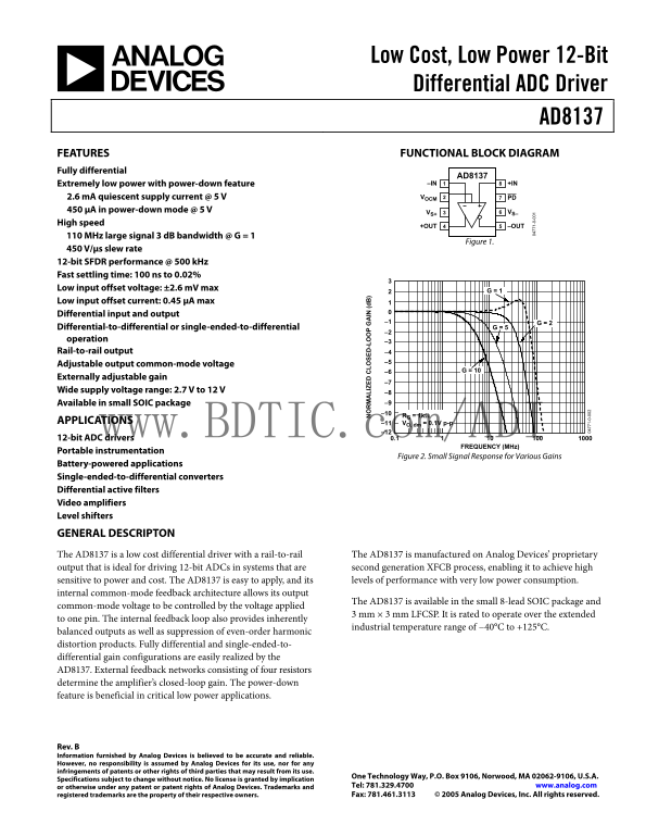
Figure 1.

450 V/µs slew rate 12-bit SFDR performance @ 500 k Hz Fast settling time: 100 ns to 0.02% Low input offset voltage: ±2.6 m V max

Low input offset current: 0.45 µA max Differential input and output

Differential-to-differential or single-ended-to-differential G = 5

operation –3 Rail-to-rail output –4

Adjustable output common-mode voltage

LI ZE G = 10 LO SE -L IN (d

Externally adjustable gain

Wide supply voltage range: 2.7 V to 12 V –8

Available in small SOIC package –9 –10 RG = 1kΩ

APPLICATIONS –11 VO, dm = 0.1V p-p

www.BDTIC.com/ADI –12 12-bit ADC drivers 0.1

FREQUENCY (MHz)

Portable instrumentation

Figure 2. Small Signal Response for Various Gains

Battery-powered applications Single-ended-to-differential converters Differential active filters Video amplifiers Level shifters

GENERAL DESCRIPTON 1- 0-

The AD8137 is a low cost differential driver with a rail-to-rail The AD8137 is manufactured on Analog Devices’ proprietary output that is ideal for driving 12-bit ADCs in systems that are second generation XFCB process, enabling it to achieve high sensitive to power and cost. The AD8137 is easy to apply, and its levels of performance with very low power consumption.

internal common-mode feedback architecture allows its output

The AD8137 is available in the small 8-lead SOIC package and

common-mode voltage to be controlled by the voltage applied

3 mm × 3 mm LFCSP. It is rated to operate over the extended

to one pin. The internal feedback loop also provides inherently

industrial temperature range of −40°C to +125°C.

balanced outputs as well as suppression of even-order harmonic distortion products. Fully differential and single-ended-to- differential gain configurations are easily realized by the AD8137. External feedback networks consisting of four resistors determine the amplifier’s closed-loop gain. The power-down feature is beneficial in critical low power applications.

Rev. B Information furnished by Analog Devices is believed to be accurate and reliable. However, no responsibility is assumed by Analog Devices for its use, nor for any infringements of patents or other rights of third parties that may result from its use.

One Technology Way, P.O. Box 9106, Norwood, MA 02062-9106, U.S.A.

Specifications subject to change without notice. No license is granted by implication

or otherwise under any patent or patent rights of Analog Devices. Trademarks and Tel: 781.329.4700 www.analog.com registered trademarks are the property of their respective owners. Fax: 781.461.3113 © 2005 Analog Devices, Inc. All rights reserved.

Page Summary Contents For AD8137 Analog Devices Data Handbook/Manual

Page 1 Low Cost, Low Power 12-Bit Differential ADC Driver AD8137 FEATURES FUNCTIONAL BLOCK DIAGRAM Fully differential AD8137 Extremely low power with power-down feature –IN +IN8 2.6 m A quiescent supply curr...
Page 2 AD8137 TABLE OF CONTENTS Specifications..................................................................................... Applications..................................................................
Page 3 AD8137 SPECIFICATIONS VS = ±5 V, VOCM = 0 V (@ 25°C, differential gain = 1, RL, dm = RF = RG = 1 kΩ, unless otherwise noted, TMIN to TMAX = −40°C to +125°C). Table 1. Parameter Conditions Min Typ Max ...
Page 4 AD8137 VS = 5 V, VOCM = 2.5 V (@ 25°C, differential gain = 1, RL, dm = RF = RG = 1 kΩ, unless otherwise noted, TMIN to TMAX = −40°C to +125°C). Table 2. Parameter Conditions Min Typ Max Unit DIFFERENT...
Page 5 AD8137 VS = 3 V, VOCM = 1.5 V (@ 25°C, differential gain = 1, RL, dm = RF = RG = 1 kΩ, unless otherwise noted, TMIN to TMAX = −40°C to +125°C). Table 3. Parameter Conditions Min Typ Max Unit DIFFERENT...
Page 6 AD8137 ABSOLUTE MAXIMUM RATINGS Table 4. Parameter Rating The power dissipated in the package (PD) is the sum of the Supply Voltage 12 V quiescent power dissipation and the power dissipated in the VOC...
Page 7 AD8137 PIN CONFIGURATION AND FUNCTION DESCRIPTIONS AD8137 –IN +IN8 VOCM PD7 VS+ VS–6 +OUT –OUT5 Figure 4. Pin Configuration Table 6. Pin Function Descriptions Pin No. Mnemonic Description 1 −IN Invert...
Page 8 LO SE -L IN (d LO SE -L IN (d LI ZE LO SE -L IN (d AD8137 TYPICAL PERFORMANCE CHARACTERISTICS Unless otherwise noted, differential gain = 1, RG = RF = RL, dm = 1 kΩ, VS = 5 V, TA = 25°C, VOCM = 2.5V. ...
Page 9 AD8137 LO SE -L IN (d LO SE -L IN (d LO SE -L IN (d RL, dm = 1kΩ RL, dm = 500Ω RL, dm = 2kΩ RL, dm = 2kΩ –9 –9 RL, dm = 500Ω RL, dm = 1kΩ –11 –11 VO, dm = 2V p-p VO, dm = 0.1V p-p FREQUENCY (MHz) FREQ...
Page 10 IS TO TI (d c) IS TO TI (d c) LO SE -L IN (d AD8137 RF = 500Ω RF = 2kΩ –3 –3 RF = 500ΩRF = 2kΩ –4 RF = 1kΩ –4 –5 –5 RF = 1kΩ –6 –6 VS ±5V G = 1 –10 VO, dm = 0.1V p-p –10 VO, dm = 2V p-p –11 –11 FREQUE...
Page 11 AD8137 IS TO TI (d c) IS TO TI (d c) IS TO TI (d c) –40 –40 VO, dm = 2V p-p VO, dm = 2V p-p RL, dm = 200Ω RL, dm = 200Ω RL, dm = 1kΩ RL, dm = 1kΩ –90 RL, dm = 500Ω –90 –100 –100 RL, dm = 500Ω FREQUENC...
Page 12 (d IN PU VO LT IS (n V/ √H z) IS TO TI (d c) AD8137 FC = 500k Hz FC = 500k Hz VO, dm = 2V p-p VO, dm = 2V p-p SECOND HARMONIC SOLID LINE SECOND HARMONIC SOLID LINE THIRD HARMONIC DASHED LINE THIRD HAR...
Page 13 AD8137 , d (V , d (m V) VO LT (V G = 2 INPUT × 2 1.5 VO, dm CF = 0p F VO, dm = 3.5V p-p OUTPUT INPUT ERROR = VO, dm - INPUT TSETTLE = 110ns 50ns/DIV 250ns/DIV TIME (ns) TIME (ns) Figure 37. Overdrive ...
Page 14 SI LE -E ED TP SW IN IL (m V) LO SE -L IN (d PS (d AD8137 –5 PSRR = ∆VO, dm/∆VS –15 –PSRR –55 +PSRR FREQUENCY (MHz) FREQUENCY (MHz) Figure 43. PSRR vs. Frequency 1- 0- Figure 46. Single-Ended Output I...
Page 15 AD8137 IA (µ S, (m V) IN PU IA EN (µ VOS, cm VOS, dm TEMPERATURE (°C) TEMPERATURE (°C) Figure 49. Offset Voltage vs. Temperature Figure 52. Supply Current vs. Temperature (µ SU PP LY EN (m EN (µ www.B...
Page 16 SU PP LY EN (m PD EN (µ , c AD8137 VS = +5V VS = ±2.5V G = 1 (RF = RG = 1kΩ) RL, dm = 1kΩ INPUT = 1Vp-p @ 1MHz VO, dm VS = +3V VS = ±5V –0.5 –4 2µs/DIV PD –2.0V VOCM TIME (µs) 1- 0- 1- Figure 58. Powe...
Page 17 AD8137 THEORY OF OPERATION The AD8137 is a low power, low cost, fully differential voltage feedback amplifier that features a rail-to-rail output stage, common-mode circuitry with an internally derive...
Page 18 AD8137 APPLICATIONS ANALYZING A TYPICAL APPLICATION WITH Output balance is measured by placing a well-matched resistor MATCHED RF AND RG NETWORKS divider across the differential voltage outputs and co...
Page 19 AD8137 The differential output voltage noise contains contributions Feedback Factor Notation from the AD8137’s input voltage noise and input current noise When working with differential drivers, it is...
Page 20 AD8137 AD8137 GND VIN AD7450A VREFB VIN+ 1kΩ 1kΩ 50Ω GND VREF +1.25VVACM WITH VREFB = 0 +0.63V 2.5V ADR525A 2.5V SHUNT VREFA REFERENCE Figure 64. AD8137 Driving AD7450A, 12-Bit A/D Converter The input...
Page 21 AD8137 Estimating DC Errors Driving a Capacitive Load Primary differential output offset errors in the AD8137 are due A purely capacitive load will react with the bondwire and pin to three major compo...
Page 22 AD8137 This example shows that when RF and RG are large compared to RT, the gain reduction produced by the increase in RG is essentially cancelled by the increase in the Thevenin voltage caused by RT ...
Page 23 AD8137 PL IT (d FU LL LE 20k Hz VDDVIN BPF VOCM 1n F AD8137 AD7687 Figure 67. AD8137 Driving AD7687, 16-Bit 250 KSPS ADC –10 THD = –91.75d Bc THD = –93.63d Bc SNR = 91.35d B SNR = 91.10d B SINAD = 88....
Page 24 AD8137 OUTLINE DIMENSIONS BSC × 45° 0.31 (0.0122)COPLANARITY 0.25 (0.0098) SEATING PLANE 0.17 (0.0067) COMPLIANT TO JEDEC STANDARDS MS-012-AA CONTROLLING DIMENSIONS ARE IN MILLIMETERS; INCH DIMENSIONS...

Manual Details

Brand Analog Devices
Pages 24
File Size 689.90 KB
Published June 15, 2026
1 views

Enter the captcha to get the download link:

captcha

Frequently Asked Questions

What is the low-power consumption feature?

It has a power-down feature, allowing very low current draw (450 µA at 5 V).

Does it support both single-ended and differential operation?

Yes. It supports fully differential output and signal conversion from single-ended to differential.

What is the operating temperature range for this device?

The industrial temperature range is −40°C to +125°C.

How can I adjust the output gain?

External feedback networks consisting of four resistors determine the amplifier’s closed-loop gain.