# A B C D E F G H I J K L M N O P Q R S T U V W X Y Z

AD7992 Analog Devices Data Handbook/Manual

Summary

This technical resource provides comprehensive documentation for the AD7992, a low-power, 12-bit successive approximation ADC with two analog input channels. The guide details its IC-compatible serial interface, fast conversion capabilities (up to 188 kSPS), and configurable operational features, including automatic shutdown and programmable out-of-range alerts. It is essential for electronics engineers developing high-performance measurement systems requiring precise, energy-efficient data acquisition processes.
📄 Preview 📖 Table of Contents Contents PAGE OF 28

Page 1 Text Content

2-Channel, 12-Bit ADC with I2C-Compatible

Interface in 10-Lead MSOP

AD7992

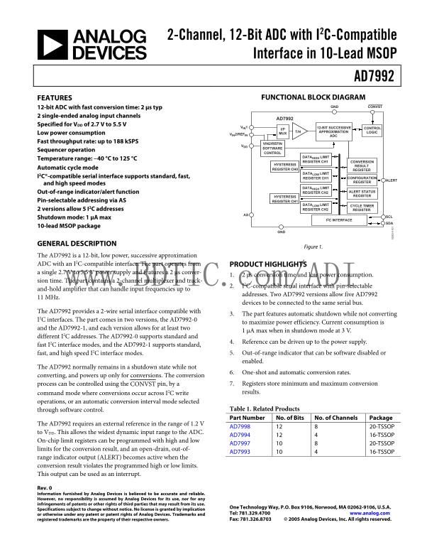
FEATURES FUNCTIONAL BLOCK DIAGRAM

12-bit ADC with fast conversion time: 2 µs typ GND CONVST

2 single-ended analog input channels

AD7992

Specified for VDD of 2.7 V to 5.5 V

VIN1 12-BIT SUCCESSIVE CONTROL

T/H APPROXIMATION LOGIC

Low power consumption VIN2/REFIN MUX

Fast throughput rate: up to 188 k SPS

VIN2/REFIN

SOFTWARE

Sequencer operation

CONTROL

DATAHIGH LIMIT

Temperature range: −40 °C to 125 °C

REGISTER CH1 CONVERSION

HYSTERESIS RESULT

Automatic cycle mode REGISTER CH0

REGISTER

DATALOW LIMIT

I2C®-compatible serial interface supports standard, fast, REGISTER CH1 CONFIGURATION

ALERT

REGISTER

and high speed modes

DATAHIGH LIMIT

Out-of-range indicator/alert function REGISTER CH2 ALERT STATUS HYSTERESIS REGISTER

Pin-selectable addressing via AS REGISTER CH1

DATALOW LIMIT CYCLE TIMER 2 versions allow 5 I2C addresses REGISTER CH2 REGISTER

Shutdown mode: 1 µA max SCL

I2C INTERFACE

10-lead MSOP package

GENERAL DESCRIPTION

Figure 1.

The AD7992 is a 12-bit, low power, successive approximation ADC with an I2C-compatible interface. The part operates from PRODUCT HIGHLIGHTS a single 2.7 V to 5.5 V power supply and features a 2 µs conver-

1. 2 µs conversion time and low power consumption.

sion time. The part contains a 2-channel multiplexer and track- www.BDTIC.c m/ADI

2. I2C-compatible serial interface with pin-selectable

and-hold amplifier that can handle input frequencies up to

addresses. Two AD7992 versions allow five AD7992

11 MHz.

devices to be connected to the same serial bus.

The AD7992 provides a 2-wire serial interface compatible with

3. The part features automatic shutdown while not converting

I2C interfaces. The part comes in two versions, the AD7992-0

to maximize power efficiency. Current consumption is

and the AD7992-1, and each version allows for at least two

1 µA max when in shutdown mode at 3 V.

different I2C addresses. The AD7992-0 supports standard and

4. Reference can be driven up to the power supply.

fast I2C interface modes, and the AD7992-1 supports standard,

fast, and high speed I2C interface modes. 5. Out-of-range indicator that can be software disabled or enabled.

The AD7992 normally remains in a shutdown state while not

6. One-shot and automatic conversion rates.

converting, and powers up only for conversions. The conversion

process can be controlled using the CONVST pin, by a 7. Registers store minimum and maximum conversion command mode where conversions occur across I2C write results. 3- 0-

operations, or an automatic conversion interval mode selected

through software control. Table 1. Related Products Part Number No. of Bits No. of Channels Package

The AD7992 requires an external reference in the range of 1.2 V

AD7998 12 8 20-TSSOP

to VDD. This allows the widest dynamic input range to the ADC.

AD7994 12 4 16-TSSOP

On-chip limit registers can be programmed with high and low

AD7997 10 8 20-TSSOP

limits for the conversion result, and an open-drain, out-of-

AD7993 10 4 16-TSSOP

range indicator output (ALERT) becomes active when the conversion result violates the programmed high or low limits. This output can be used as an interrupt.

Rev. 0 Information furnished by Analog Devices is believed to be accurate and reliable. However, no responsibility is assumed by Analog Devices for its use, nor for any infringements of patents or other rights of third parties that may result from its use.

One Technology Way, P.O. Box 9106, Norwood, MA 02062-9106, U.S.A.

Specifications subject to change without notice. No license is granted by implication

or otherwise under any patent or patent rights of Analog Devices. Trademarks and Tel: 781.329.4700 www.analog.com registered trademarks are the property of their respective owners. Fax: 781.326.8703 © 2005 Analog Devices, Inc. All rights reserved.

Page Summary Contents For AD7992 Analog Devices Data Handbook/Manual

Page 1 2-Channel, 12-Bit ADC with I2C-Compatible Interface in 10-Lead MSOP AD7992 FEATURES FUNCTIONAL BLOCK DIAGRAM 12-bit ADC with fast conversion time: 2 µs typ GND CONVST 2 single-ended analog input chann...
Page 2 AD7992 TABLE OF CONTENTS Specifications..................................................................................... Serial Interface I2C Timing Specifications Serial Bus Address.................
Page 3 AD7992 SPECIFICATIONS Temperature range for B version is −40°C to +125°C. Unless otherwise noted, VDD = 2.7 V to 5.5 V; REFIN = 2.5 V to VDD. For the AD7992-0, all specifications apply for f SCL up to...
Page 4 AD7992 Parameter B Version Unit Test Conditions/Comments LOGIC INPUTS (CONVST) Input High Voltage, VINH 2.4 V min VDD = 5 V 2.0 V min VDD = 3 V Input Low Voltage, VINL 0.8 V max VDD = 5 V 0.4 V max VD...
Page 5 AD7992 I2C TIMING SPECIFICATIONS Guaranteed by initial characterization. All values measured with the input filtering enabled. CB refers to the capacitive load on the bus line. tr and tf measured betw...
Page 6 AD7992 Limit at TMIN, TMAX Parameter Conditions Min Max Unit Description t10 Standard mode 300 ns t FDA, fall time of SDA signal Fast mode 20 + 0.1 CB 300 ns High speed mode CB = 100 p F max 10 80 ns ...
Page 7 AD7992 ABSOLUTE MAXIMUM RATINGS TA = 25°C, unless otherwise noted. Table 4. Stresses above those listed under Absolute Maximum Ratings Parameter Rating may cause permanent damage to the device. This i...
Page 8 AD7992 PIN CONFIGURATION AND PIN FUNCTION DESCRIPTIONS CONVST SCL AGND SDA VDD AD7992 ALERT VIN2/REFIN TOP VIEW AGND (Not to Scale) ASVIN1 Figure 3. AD7992 Pin Configuration Table 5. Pin Function Desc...
Page 9 AD7992 TERMINOLOGY Signal-to-Noise and Distortion Ratio (SINAD) Channel-to-Channel Isolation The measured ratio of signal-to-noise and distortion at the A measure of the level of crosstalk between cha...
Page 10 PS (d SI (d SI (d AD7992 TYPICAL PERFORMANCE CHARACTERISTICS FS = 121k SPS VDD = 5.0V VDD = 4.5V FSCL = 3.4MHz FIN = 10k Hz –20 VDD = 5.5V SNR = 71.84d B SINAD = 71.68d B THD = –86.18d B –40 SFDR = –8...
Page 11 AD7992 IN ER (L SB ER (L SB IN ER (L SB 0.4 0.4 POSITIVE DNL NEGATIVE DNL CODE REFERENCE VOLTAGE (V) Figure 10. Typical INL, VDD = 2.7 V, Reference = 2.5 V, Mode1, Figure 13. Change in DNL vs. Referen...
Page 12 EN (B IT S) AD7992 12.0 ENOB VDD = 5V ENOB VDD = 3V 11.6 SINAD VDD = 5V SINAD VDD = 3V REFERENCE VOLTAGE (V) SI (d Figure 16. ENOB/SINAD vs. Reference Voltage, Mode 1, 121 k SPS www.BDTIC.com/ADI Rev....
Page 13 AD7992 CIRCUIT INFORMATION The AD7992 is a low power, 12-bit, single-supply, 2-channel When the ADC starts a conversion, as shown in Figure 18, analog-to-digital converter (ADC). The part can be opera...
Page 14 AD7992 TYPICAL CONNECTION DIAGRAM ANALOG INPUT Figure 21 shows the typical connection diagram for the Figure 20 shows an equivalent circuit of the AD7992 analog AD7992. In Figure 21, the address selec...
Page 15 AD7992 VREF = 2.5V For ac applications, removing high frequency components from the analog input signal is recommended by use of an RC band- pass filter on the relevant analog input pin. In applicatio...
Page 16 AD7992 INTERNAL REGISTER STRUCTURE ADDRESS POINTER REGISTER The AD7992 contains 11 internal registers (see Figure 24) that Because it is the register to which the first data byte of every are used to ...
Page 17 AD7992 CONFIGURATION REGISTER The configuration register is a 8-bit, read/write register that is used to set the operating modes of the AD7992. The MSB of the register is unused and is a don’t care bi...
Page 18 AD7992 CONVERSION RESULT REGISTER The conversion result register is a 16-bit, read-only register that reset. The value of N is taken from the 12-bit hysteresis register stores the conversion result fr...
Page 19 AD7992 Using the Limit Registers to Store Min/Max Conversion CYCLE TIMER REGISTER Results The cycle timer register is an 8-bit read/write register that stores If full scale—that is, all 1s—is written ...
Page 20 AD7992 SERIAL INTERFACE Control of the AD7992 is carried out via the I2C-compatible Data is sent over the serial bus in sequences of nine clock serial bus. The AD7992 is connected to this bus as a sla...
Page 21 AD7992 WRITING TO THE AD7992 Depending on the register being written to, there are three WRITING A SINGLE BYTE OF DATA TO THE ALERT different writes for the AD7992. STATUS REGISTER, CYCLE REGISTER, OR...
Page 22 AD7992 WRITING TWO BYTES OF DATA TO A LIMIT REGISTER OR HYSTERESIS REGISTER Each of the limit registers and hysteresis registers are 12-bit If the master is write-addressing the AD7992, it can write t...
Page 23 AD7992 READING DATA FROM THE AD7992 Reading data from the AD7992 is a 1- or 2-byte operation. Reading data from the conversion result register, DATAHIGH Reading back the contents of the alert status r...
Page 24 AD7992 ALERT/BUSY PIN The ALERT/BUSY pin may be configured as an ALERT output The ALERT output requires an external pull-up resistor that or BUSY output, as shown in Table 11. can be connected to a vo...
Page 25 AD7992 MODES OF OPERATION When supplies are first applied to the AD7992, the ADC If the CONVST pulse does not remain high for more than 1 µs, powers up in sleep mode and normally remains in this the f...
Page 26 AD7992 MODE 2 – COMMAND MODE Mode 2 allows a conversion to be automatically initiated any accesses the data from the conversion on VIN1. While this read time a write operation occurs. In order to use ...
Page 27 AD7992 COMMAND/ADDRESS 7-BIT ADDRESS POINT BYTE ACK BY ACK BY AD7992 AD7992 FIRST DATA BYTE SECOND DATA BYTE FIRST DATA BYTE SECOND DATA BYTE 7-BIT ADDRESS (LSBs) (MSBs) (LSBs)ASr A/A (MSBs) ACK BY AC...
Page 28 AD7992 OUTLINE DIMENSIONS 3.00 BSC 4.90 BSC 3.00 BSC PIN 1 0.50 BSC 0.95 0.85 1.10 MAX 0.75 SEATING 0.60 0.00 0.17 PLANE 0.08 0.40 COPLANARITY 0.10 COMPLIANT TO JEDEC STANDARDS MO-187BA Figure 34. 10-...

Manual Details

Brand Analog Devices
Pages 28
File Size 776.83 KB
Published June 16, 2026
1 views

Enter the captcha to get the download link:

captcha

Frequently Asked Questions

What is the typical conversion time for this ADC?

The AD7992 features a fast conversion time of 2 µs typ.

How can I detect if the input voltage is out of range?

An open-drain ALERT output activates when the conversion result violates programmed high or low limits.

How many devices can be connected to the same serial bus using this chip?

It enters an automatic shutdown mode, consuming a maximum of 1 µA current.