AD7765 Analog Devices Data Handbook & Manual
Summary
This high-performance 24-bit Σ-Δ Analog-to-Digital Converter (ADC) is engineered for critical data acquisition in demanding environments. Featuring integrated FIR filtering, differential buffering, and low power modes, it minimizes the need for extensive external signal conditioning. The accompanying documentation guides users through advanced system integration, covering topics like synchronization protocols, customizable decimation rates, and precise overrange management. It is an ideal resource for electrical engineers designing high-accuracy instrumentation, vibration analysis equipment, and complex industrial monitoring systems.
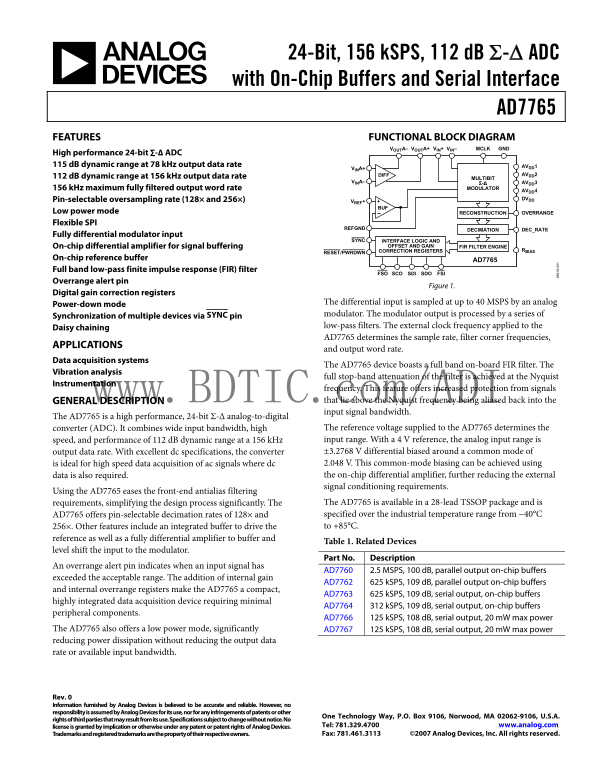
Page 1 Text Content
24-Bit, 156 k SPS, 112 d B Σ-Δ ADC with On-Chip Buffers and Serial Interface
AD7765 FEATURES FUNCTIONAL BLOCK DIAGRAM
VOUTA– VOUTA+ VIN+ VIN– MCLK GND
High performance 24-bit ∑-∆ ADC 115 d B dynamic range at 78 k Hz output data rate AVDD1
VINA+
DIFF AVDD2
112 d B dynamic range at 156 k Hz output data rate MULTIBIT
VINA– Σ-Δ AVDD3
156 k Hz maximum fully filtered output word rate MODULATOR
AVDD4 Pin-selectable oversampling rate (128× and 256×) DVDD
VREF+
Low power mode RECONSTRUCTION OVERRANGE Flexible SPI
REFGND DECIMATION DEC_RATE
Fully differential modulator input
SYNC INTERFACE LOGIC AND
On-chip differential amplifier for signal buffering OFFSET AND GAIN FIR FILTER ENGINE
CORRECTION REGISTERS RBIAS
RESET/PWRDWN
On-chip reference buffer AD7765 Full band low-pass finite impulse response (FIR) filter
FSO SCO SDI SDO FSI
Overrange alert pin
Figure 1.
Digital gain correction registers
The differential input is sampled at up to 40 MSPS by an analog
Power-down mode
modulator. The modulator output is processed by a series of
Synchronization of multiple devices via SYNC pin
Daisy chaining low-pass filters. The external clock frequency applied to the AD7765 determines the sample rate, filter corner frequencies,
APPLICATIONS
and output word rate.
Data acquisition systems
The AD7765 device boasts a full band on-board FIR filter. The
Vibration analysis
full stop-band attenuation of the filter is achieved at the Nyquist
Instrumentation
frequency. This feature offers increased protection from signals GENERAL DESCRIPTION www.BDTIC.c that lie above the Nyquist frequency being aliased back into the m/ADI input signal bandwidth.
The AD7765 is a high performance, 24-bit Σ-Δ analog-to-digital
converter (ADC). It combines wide input bandwidth, high The reference voltage supplied to the AD7765 determines the speed, and performance of 112 d B dynamic range at a 156 k Hz input range. With a 4 V reference, the analog input range is output data rate. With excellent dc specifications, the converter ±3.2768 V differential biased around a common mode of is ideal for high speed data acquisition of ac signals where dc 2.048 V. This common-mode biasing can be achieved using data is also required. the on-chip differential amplifier, further reducing the external signal conditioning requirements.
Using the AD7765 eases the front-end antialias filtering
requirements, simplifying the design process significantly. The The AD7765 is available in a 28-lead TSSOP package and is AD7765 offers pin-selectable decimation rates of 128× and specified over the industrial temperature range from −40°C 256×. Other features include an integrated buffer to drive the to +85°C.
reference as well as a fully differential amplifier to buffer and
Table 1. Related Devices
level shift the input to the modulator.
Part No. Description 9-
An overrange alert pin indicates when an input signal has
AD7760 2.5 MSPS, 100 d B, parallel output on-chip buffers
exceeded the acceptable range. The addition of internal gain
AD7762 625 k SPS, 109 d B, parallel output on-chip buffers
and internal overrange registers make the AD7765 a compact,
AD7763 625 k SPS, 109 d B, serial output, on-chip buffers
highly integrated data acquisition device requiring minimal
AD7764 312 k SPS, 109 d B, serial output, on-chip buffers
peripheral components.
AD7766 125 k SPS, 108 d B, serial output, 20 m W max power
The AD7765 also offers a low power mode, significantly AD7767 125 k SPS, 108 d B, serial output, 20 m W max power reducing power dissipation without reducing the output data rate or available input bandwidth.
Rev. 0 Information furnished by Analog Devices is believed to be accurate and reliable. However, no responsibility is assumed by Analog Devices for its use, nor for any infringements of patents or other
One Technology Way, P.O. Box 9106, Norwood, MA 02062-9106, U.S.A.
rights of third parties that may result from its use. Specifications subject to change without notice. No
license is granted by implication or otherwise under any patent or patent rights of Analog Devices. Tel: 781.329.4700 www.analog.com Trademarks and registered trademarks are the property of their respective owners. Fax: 781.461.3113 ©2007 Analog Devices, Inc. All rights reserved.
Page Summary Contents For AD7765 Analog Devices Data Handbook & Manual
Manual Details
| Brand | Analog Devices |
|---|---|
| Pages | 32 |
| File Size | 1018.51 KB |
| Published | June 15, 2026 |
Enter the captcha to get the download link:

Frequently Asked Questions
What is the device's high-frequency protection against aliasing?
The AD7765 includes a full band on-board FIR filter which offers protection from signals lying above the Nyquist frequency.
How do I know if my input signal exceeds the acceptable range?
The overrange alert pin activates when the analog input voltage exceeds 100% of VREF for more than four consecutive samples.
What is the typical operating temperature range?
The AD7765 operates within the industrial temperature range from −40°C to +85°C.
Does this device support varying data acquisition rates?
Yes, it offers pin-selectable decimation rates of 128× and 256×.