AD7482 ANALOG DEVICES Data Handbook/Manual
Summary
This AD7482 is a high-speed, 12-bit Successive Approximation Register (SAR) ADC designed for precise signal acquisition. It offers impressive performance at up to 3 MSPS with ample bandwidth and advanced features like algorithmic offset removal and native support for overrange input via the 13th bit. With excellent low-power modes, it is ideal for designers building sophisticated data logging or instrumentation systems. The manual provides comprehensive technical coverage, including detailed operational theory, timing diagrams, power saving methods, and interface specifications, ensuring engineers have all necessary details for high-fidelity signal processing applications.
Page 1 Text Content
3 MSPS, 12-Bit SAR ADC
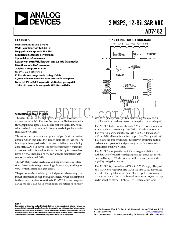
AD7482 FEATURES FUNCTIONAL BLOCK DIAGRAM
AVDD AGND CBIAS DVDD VDRIVE DGND
Fast throughput rate: 3 MSPS Wide input bandwidth: 40 MHz No pipeline delays with SAR ADC
BUF REFOUT
Excellent dc accuracy performance REFERENCE
2 parallel interface modes REFSEL REFIN
Low power: 90 m W (full power) and 2.5 m W (nap mode) Standby mode: 2 μA maximum 12-BIT
ALGORITHMIC
Single 5 V supply operation VIN T/H SAR Internal 2.5 V reference
Full-scale overrange mode (using 13th bit) AD7482
System offset removal via user access offset register
MODE1
Nominal 0 V to 2.5 V input with shifted range capability D11
MODE2
14-bit pin compatible upgrade AD7484 available CLIP CONTROL
NAP LOGIC AND I/O
REGISTERS D8
RESET
CONVST
Figure 1.
GENERAL DESCRIPTION www.BDTIC.com/ADI
The AD7482 is a 12-bit, high speed, low power, successive alive for a quick power-up while consuming 2.5 m W, and a approximation ADC. The part features a parallel interface with standby mode that reduces power consumption to a mere 10 μW.
throughput rates up to 3 MSPS. The part contains a low noise, IT
The AD7482 features an on-board 2.5 V reference but can also
wide bandwidth track-and-hold that can handle input frequencies
accommodate an externally provided 2.5 V reference source.
in excess of 40 MHz.
The nominal analog input range is 0 V to 2.5 V, but an offset The conversion process is a proprietary algorithmic successive shift capability allows this nominal range to be offset by ±200 m V. approximation technique that results in no pipeline delays. The This allows the user considerable flexibility in setting the bottom input signal is sampled, and a conversion is initiated on the falling end reference point of the signal range, a useful feature when edge of the CONVST signal. The conversion process is controlled using single-supply op amps.
via an internally trimmed oscillator. Interfacing is via standard
The AD7482 also provides an 8% overrange capability via a
parallel signal lines, making the part directly compatible with
13th bit. Therefore, if the analog input range strays outside the 8-
microcontrollers and DSPs.
nominal by up to 8%, the user can still accurately resolve the The AD7482 provides excellent ac and dc performance specifica- signal by using the 13th bit.
tions. Factory trimming ensures high dc accuracy, resulting in
The AD7482 is powered by a 4.75 V to 5.25 V supply. The part
very low INL, offset, and gain errors.
also provides a VDRIVE pin that allows the user to set the voltage The part uses advanced design techniques to achieve very low levels for the digital interface lines. The range for this VDRIVE pin power dissipation at high throughput rates. Power consumption is 2.7 V to 5.25 V. The part is housed in a 48-lead LQFP package in the normal mode of operation is 90 m W. There are two power and is specified over a −40°C to +85°C temperature range.
saving modes: a nap mode, which keeps the reference circuitry
Rev. A Information furnished by Analog Devices is believed to be accurate and reliable. However, no responsibility is assumed by Analog Devices for its use, nor for any infringements of patents or other
One Technology Way, P.O. Box 9106, Norwood, MA 02062-9106, U.S.A.
rights of third parties that may result from its use. Specifications subject to change without notice. No
license is granted by implication or otherwise under any patent or patent rights of Analog Devices. Tel: 781.329.4700 www.analog.com Trademarks and registered trademarks are the property of their respective owners. Fax: 781.461.3113 ©2002–2008 Analog Devices, Inc. All rights reserved.
Page Summary Contents For AD7482 ANALOG DEVICES Data Handbook/Manual
Manual Details
| Brand | Analog Devices |
|---|---|
| Pages | 20 |
| File Size | 603.64 KB |
| Published | June 15, 2026 |
Enter the captcha to get the download link:

Frequently Asked Questions
What voltage do I need to power the AD7482 ADC?
The AD7482 is powered by a 4.75 V to 5.25 V supply.
How can I handle analog signals that exceed the nominal 0V to 2.5V input range?
It provides an 8% overrange capability using the 13th bit, allowing resolution up to 3.25V.
What power-saving modes are available for the device?
The AD7482 has two low-power modes: Nap mode and standby mode (maximum consumption is 2 μA).
How fast can the ADC handle input signals?
It features a high throughput rate of up to 3 MSPS.