AD7451 Analog Devices Data Handbook/Manual
Summary
These high-speed, low-power SAR ADCs are engineered for mission-critical data acquisition systems and portable instrumentation relying on battery power. Featuring pseudo differential inputs and a throughput of up to 1 MSPS, they deliver exceptional performance with minimal power consumption while operating from a single supply. This resource provides comprehensive technical details covering functional block diagrams, operational modes, flexible clock synchronization, and integration guidelines for robust system design.
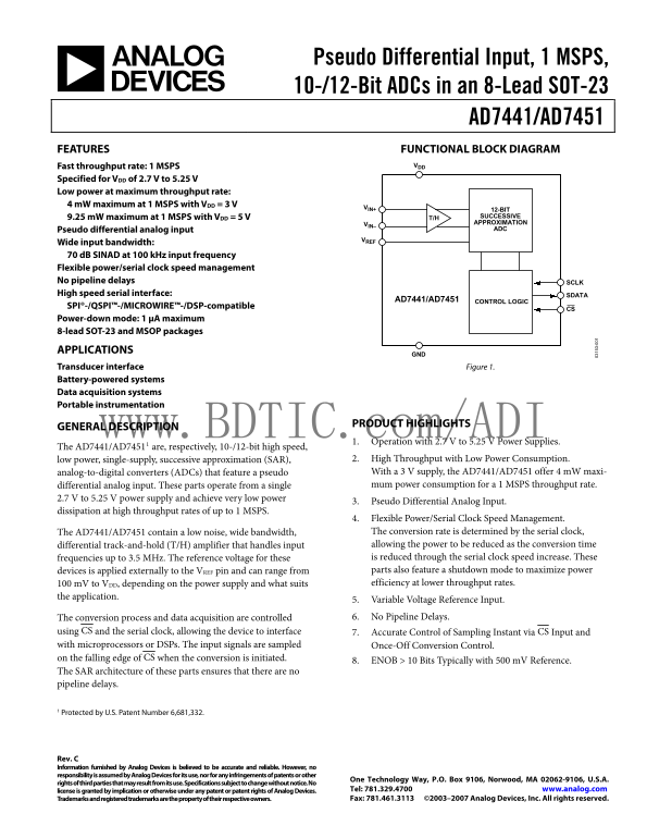
Page 1 Text Content
Pseudo Differential Input, 1 MSPS, 10-/12-Bit ADCs in an 8-Lead SOT-23
AD7441/AD7451 FEATURES FUNCTIONAL BLOCK DIAGRAM
Fast throughput rate: 1 MSPS VDD
Specified for VDD of 2.7 V to 5.25 V Low power at maximum throughput rate: 4 m W maximum at 1 MSPS with VDD = 3 V
12-BIT 9.25 m W maximum at 1 MSPS with VDD = 5 V T/H SUCCESSIVE VIN– APPROXIMATION Pseudo differential analog input ADC
Wide input bandwidth: 70 d B SINAD at 100 k Hz input frequency Flexible power/serial clock speed management No pipeline delays SCLK High speed serial interface: SDATA
AD7441/AD7451 CONTROL LOGIC
SPI®-/QSPI™-/MICROWIRE™-/DSP-compatible
Power-down mode: 1 μA maximum 8-lead SOT-23 and MSOP packages
APPLICATIONS
Transducer interface Figure 1.
Battery-powered systems Data acquisition systems Portable instrumentation
PRODUCT HIGHLIGHTS
GENERAL DESCRIPTION www.BDTIC.com/ADI
1. Operation with 2.7 V to 5.25 V Power Supplies.
The AD7441/AD74511 are, respectively, 10-/12-bit high speed,
low power, single-supply, successive approximation (SAR), 2. High Throughput with Low Power Consumption. analog-to-digital converters (ADCs) that feature a pseudo With a 3 V supply, the AD7441/AD7451 offer 4 m W maxi- differential analog input. These parts operate from a single mum power consumption for a 1 MSPS throughput rate.
2.7 V to 5.25 V power supply and achieve very low power
3. Pseudo Differential Analog Input.
dissipation at high throughput rates of up to 1 MSPS.
4. Flexible Power/Serial Clock Speed Management. The AD7441/AD7451 contain a low noise, wide bandwidth, The conversion rate is determined by the serial clock, differential track-and-hold (T/H) amplifier that handles input allowing the power to be reduced as the conversion time frequencies up to 3.5 MHz. The reference voltage for these is reduced through the serial clock speed increase. These devices is applied externally to the VREF pin and can range from parts also feature a shutdown mode to maximize power 100 m V to VDD, depending on the power supply and what suits efficiency at lower throughput rates.
the application. 3-
5. Variable Voltage Reference Input. The conversion process and data acquisition are controlled 6. No Pipeline Delays.
using CS and the serial clock, allowing the device to interface 7. Accurate Control of Sampling Instant via CS Input and with microprocessors or DSPs. The input signals are sampled Once-Off Conversion Control. on the falling edge of CS when the conversion is initiated.
8. ENOB > 10 Bits Typically with 500 m V Reference.
The SAR architecture of these parts ensures that there are no pipeline delays.
1 Protected by U.S. Patent Number 6,681,332.
Rev. C Information furnished by Analog Devices is believed to be accurate and reliable. However, no responsibility is assumed by Analog Devices for its use, nor for any infringements of patents or other
One Technology Way, P.O. Box 9106, Norwood, MA 02062-9106, U.S.A.
rights of third parties that may result from its use. Specifications subject to change without notice. No
license is granted by implication or otherwise under any patent or patent rights of Analog Devices. Tel: 781.329.4700 www.analog.com Trademarks and registered trademarks are the property of their respective owners. Fax: 781.461.3113 ©2003–2007 Analog Devices, Inc. All rights reserved.
Page Summary Contents For AD7451 Analog Devices Data Handbook/Manual
Manual Details
| Brand | Analog Devices |
|---|---|
| Pages | 24 |
| File Size | 647.08 KB |
| Published | June 05, 2026 |
Enter the captcha to get the download link:

Frequently Asked Questions
What is the power supply range for these ADCs?
They operate from a single 2.7 V to 5.25 V power supply.
How does the device handle low power consumption at high throughput?
At 1 MSPS with V = 3 V, they consume only 4 mW maximum power.
Which inputs are supported for data acquisition?
The ADCs support a pseudo differential analog input and can interface via SPI®, QSPI™, MICROWIRE™, or DSP-compatible serial interfaces.
How is the sampling instant controlled during conversion?
Input signals are sampled on the falling edge of CS when the conversion is initiated.