AD7356 Analog Devices Data Sheet
Summary
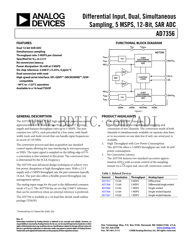
The AD7356 is a sophisticated dual, 12-bit SAR ADC designed for high-speed, low-power data acquisition up to 5 MSPS. It enables simultaneous sampling of two channels from a single 2.5V supply, minimizing complexity while maintaining precision. This manual provides comprehensive technical details, including architectural block diagrams, operational modes (Normal and Power-Down), and detailed specifications necessary for rigorous AC/DC performance evaluation. Ideal for electrical engineers developing advanced instrumentation or monitoring systems requiring reliable, high-throughput dual-channel analog input measurement.
Page 1 Text Content
Differential Input, Dual, Simultaneous Sampling, 5 MSPS, 12-Bit, SAR ADC
AD7356 FEATURES FUNCTIONAL BLOCK DIAGRAM
VDRIVEVDD
Dual 12-bit SAR ADC Simultaneous sampling
AD7356
Throughput rate: 5 MSPS per channel
VINA+
12-BIT
Specified for VDD at 2.5 V T/H
SUCCESSIVE
VINA– SDATAA
APPROXIMATION
No conversion latency ADC
Power dissipation: 36 m W at 5 MSPS On-chip reference: 2.048 V ± 0.25%, 6 ppm/°C
Dual conversion with read
High speed serial interface: SPI-/QSPI™-/MICROWIRE™-/DSP- CONTROL
LOGIC
compatible
−40°C to +125°C operation Available in a 16-lead TSSOP
12-BIT SUCCESSIVE
VINB+ SDATAB
APPROXIMATION
VINB–
AGND DGNDREFGNDAGND
Figure 1.
GENERAL DESCRIPTION PRODUCT HIGHLIGHTS The AD73561 is a dual, 12-bit, high speed, low power, successive 1. Two Complete ADC Functions. approximation ADC that operates from a single 2.5 V power www.BDTIC.com/ADI These functions allow simultaneous sampling and supply and features throughput rates up to 5 MSPS. The part conversion of two channels. The conversion result of both contains two ADCs, each preceded by a low noise, wide band- channels is simultaneously available on separate data lines width track-and-hold circuit that can handle input frequencies or in succession on one data line if only one serial port is in excess of 110 MHz. available.
2. High Throughput with Low Power Consumption.
The conversion process and data acquisition use standard
The AD7356 offers a 5 MSPS throughput rate with 36 m W
control inputs allowing for easy interfacing to microprocessors
power consumption.
or DSPs. The input signal is sampled on the falling edge of CS;
3. No Conversion Latency.
a conversion is also initiated at this point. The conversion time
The AD7356 features two standard successive approx-
is determined by the SCLK frequency.
imation ADCs with accurate control of the sampling
The AD7356 uses advanced design techniques to achieve very
instant via a CS input and, once off, conversion control.
low power dissipation at high throughput rates. With a 2.5 V supply and a 5 MSPS throughput rate, the part consumes typically
Table 1. Related Devices
14 m A. The part also offers a flexible power/throughput rate
Generic Resolution Throughput Analog Input
management option.
AD7352 12-bit 3 MSPS Differential The analog input range for the part is the differential common AD7266 12-bit 2 MSPS Differential/single ended mode ±VREF/2. The AD7356 has an on-chip 2.048 V reference AD7866 12-bit 1 MSPS Single-ended that can be overdriven when an external reference is preferred. AD7366 12-bit 1 MSPS Single-ended bipolar AD7367 14-bit 1 MSPS Single-ended bipolar
The AD7356 is available in a 16-lead thin shrink small outline package (TSSOP).
1 Protected by U.S. Patent No. 6,681,332.
Rev. 0 Information furnished by Analog Devices is believed to be accurate and reliable. However, no responsibility is assumed by Analog Devices for its use, nor for any infringements of patents or other
One Technology Way, P.O. Box 9106, Norwood, MA 02062-9106, U.S.A.
rights of third parties that may result from its use. Specifications subject to change without notice. No
license is granted by implication or otherwise under any patent or patent rights of Analog Devices. Tel: 781.329.4700 www.analog.com Trademarks and registered trademarks are the property of their respective owners. Fax: 781.461.3113 ©2008 Analog Devices, Inc. All rights reserved.
Page Summary Contents For AD7356 Analog Devices Data Sheet
Manual Details
| Brand | Analog Devices |
|---|---|
| Pages | 20 |
| File Size | 503.10 KB |
| Published | June 16, 2026 |
Enter the captcha to get the download link:

Frequently Asked Questions
What does the AD7356 offer in terms of sampling and conversion?
It is a dual, 12-bit SAR ADC designed for simultaneous sampling, allowing both channels to be processed concurrently.
Does this ADC have any conversion latency when converting data?
No, it features no conversion latency; the conversion process begins immediately upon sampling at the falling edge of the clock input.
What is the maximum throughput and typical power consumption?
It offers a 5 MSPS throughput rate, consuming typically 36 mW when operating with a 2.5 V supply.
What package and temperature ranges are available for this model?
The AD7356 can be found in a 16-lead TSSOP package and is available in versions rated up to +125°C.