Vishay SiC769CD User Guide
Summary
The SiC769CD is an advanced integrated DrMOS Power Stage and Gate Driver solution optimized for high efficiency in multi-phase core voltage regulation systems. This component integrates specialized MOSFETs and a robust driver IC, enabling efficiencies over 90% at frequencies exceeding 1 MHz. The manual details its sophisticated features, including adaptive dead time control, Automatic Skip Mode (SMOD), and comprehensive protection mechanisms (UVLO, shoot-through). It is the preferred solution for electrical engineers designing high-performance power supplies in servers, workstations, and graphics hardware.
Page 1 Text Content
Si C769CD Vishay Siliconix
Integrated Dr MOS Power Stage
DESCRIPTION FEATURES The Si C769CD is an integrated solution that contains PWM Integrated Gen III MOSFETs and Dr MOS optimized n-channel MOSFETs (high side and low side) and compliant gate driver IC a full featured MOSFET driver IC. The device complies with Enables Vcore switching at 1 MHz
the Intel Dr MOS standard for desktop and server Vcore power Easily achieve > 90 % efficiency in multi-phase, stages. The Si C769CD delivers up to 35 A continuous output low output voltage solutions current and operates from an input voltage range of 3 V to Low ringing on the VSWH pin reduces EMI 16 V. The integrated MOSFETs are optimized for output
Pin compatible with Dr MOS 6 x 6 version 3.0
voltages in the ranges of 0.8 V to 2.0 V with a nominal input
Tri-state PWM input function prevents negative output
voltage of 12 V. The device can also deliver very high power
voltage swing
at 5 V output for ASIC applications.
5 V logic levels on PWM
The Si C769CD incorporates an advanced MOSFET gate
MOSFET threshold voltage optimized for 5 V driver bias
driver IC. This IC accepts a single PWM input from the VR
supply IN
controller and converts it into the high side and low side
Automatic skip mode operation (SMOD) for light load
MOSFET gate drive signals. The driver IC is designed to
efficiency
implement the skip mode (SMOD) function for light load
Under-voltage lockout
efficiency improvement. Adaptive dead time control also
Built-in bootstrap schottky diode
works to improve efficiency at all load points. The Si C769CD ate D river
has a thermal warning (THDN) that alerts the system of Adaptive deadtime and shoot through protection excessive junction temperature. The driver IC includes an Thermal shutdown warning flag enable pin, UVLO and shoot through protection. Low profile, thermally enhanced Power PAK® MLP 6 x 6 The Si C769CD is optimized for high frequency buck 40 pin package applications. Operating frequencies in excess of 1 MHz can Halogen-free according to IEC 61249-2-21 definition
easily be achieved. Compliant to Ro HS directive 2002/95/EC The Si C769CD is packaged in Vishay Siliconix high performance Power PAK MLP6 x 6 package. Compact APPLICATIONS co-packaging of components helps to reduce stray
CPU and GPU core voltage regulation
inductance, and hence increases efficiency.
Server, computer, workstation, game console, graphics boards, PC
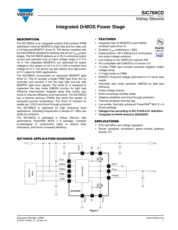
Si C769CD APPLICATION DIAGRAMM
VIN5 V
ontroller
SMOD BOOT
DSBL# VSWH
PHASE
Si C769CD
Figure 1
Document Number: 64981 www.vishay.com S10-0113-Rev. D, 18-Jan-10
Page Summary Contents For Vishay SiC769CD User Guide
Manual Details
| Brand | Vishay |
|---|---|
| Pages | 16 |
| File Size | 382.93 KB |
| Published | May 28, 2026 |
Enter the captcha to get the download link:
