Vishay FCSP240LTR User Guide
Summary
Seeking a high-performance, space-saving rectifier? This Schottky diode utilizes advanced wafer-level chip scale packaging to deliver ultra-low voltage drop and maximum efficiency in minimal board real estate. Ideal for designers creating portable electronics, such as cell phones, MP3 players, and GPS units, the compact design drastically reduces thermal resistance. The associated manual provides comprehensive technical specifications, including detailed electrical and thermal ratings necessary for reliable circuit integration.
Page 1 Text Content
FCSP240LTR
Vishay High Power Products
Flip KY®
Chip Scale Package Schottky Barrier Rectifier
FEATURES Ultra low VF per footprint area Low leakage
Low thermal resistance Ro HS COMPLIANT
One-fifth footprint of SMA Super low profile (0.6 mm) Available tested on tape and reel
APPLICATIONS Reverse polarity protection
Flip KY®
Current steering Freewheeling Flyback Oring
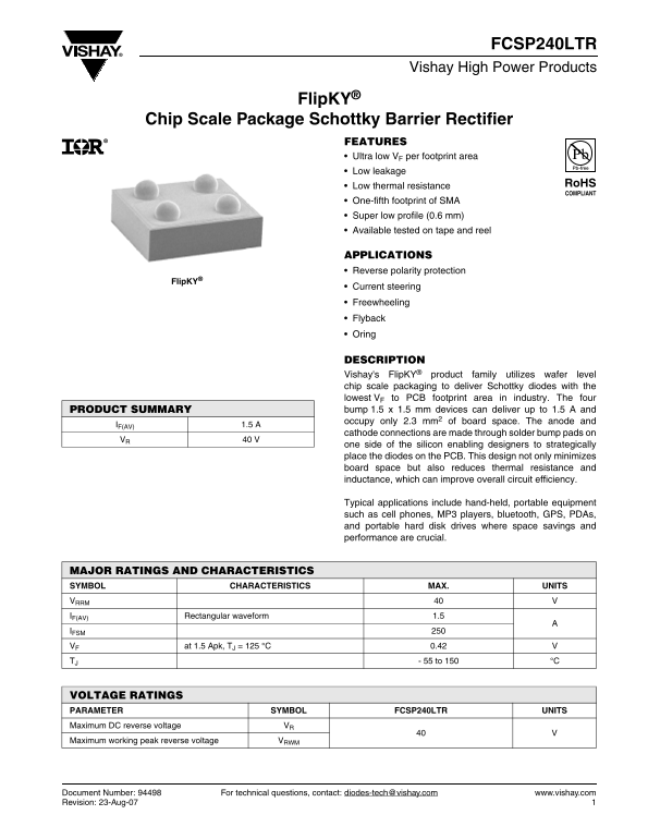
DESCRIPTION Vishay's Flip KY® product family utilizes wafer level chip scale packaging to deliver Schottky diodes with the lowest VF to PCB footprint area in industry. The four PRODUCT SUMMARY bump 1.5 x 1.5 mm devices can deliver up to 1.5 A and occupy only 2.3 mm2 of board space. The anode and
IF(AV) 1.5 A
cathode connections are made through solder bump pads on
VR 40 V
one side of the silicon enabling designers to strategically place the diodes on the PCB. This design not only minimizes board space but also reduces thermal resistance and inductance, which can improve overall circuit efficiency.
Typical applications include hand-held, portable equipment such as cell phones, MP3 players, bluetooth, GPS, PDAs, and portable hard disk drives where space savings and performance are crucial.
MAJOR RATINGS AND CHARACTERISTICS SYMBOL CHARACTERISTICS MAX. UNITS VRRM IF(AV) Rectangular waveform 1.5 IFSM VF at 1.5 Apk, TJ = 125 °C 0.42 TJ - 55 to 150 °C
VOLTAGE RATINGS PARAMETER SYMBOL FCSP240LTR UNITS Maximum DC reverse voltage VR Maximum working peak reverse voltage VRWM
Document Number: 94498 For technical questions, contact: [email protected] www.vishay.com
Revision: 23-Aug-07
Page Summary Contents For Vishay FCSP240LTR User Guide
Manual Details
| Brand | Vishay |
|---|---|
| Pages | 6 |
| File Size | 108.51 KB |
| Published | May 28, 2026 |
Enter the captcha to get the download link:

Frequently Asked Questions
What are the recommended applications for this rectifier?
It is suitable for hand-held and portable equipment such as cell phones, MP3 players, GPS, or PDAs where space efficiency is critical.
How does the chip scale package reduce board size?
The design minimizes board space by enabling connections via solder bump pads on one side of the silicon, occupying only 2.3 mm of board space.
What do I need to consider regarding heat dissipation?
Thermal resistance is important; note that total power dissipation includes both forward and inverse losses (Pd + Pd) when calculating junction temperature.
What are the maximum voltage ratings for this component?
The document specifies a Maximum DC reverse voltage ($V_{RRM}$) of 40 V and a Maximum working peak reverse voltage ($V_{RWM}$).