Philips Semiconductors 8-bit Parallel-Access Shift Register 74F199 User Manual and Technical Specifications
Summary
The 74F199 is a high-speed 8-bit Parallel Access Shift Register designed for critical data handling in digital circuits. It excels at performing synchronous, bit-accurate transfers via both shift-right and parallel load modes. This manual provides comprehensive technical specifications for hardware engineers, detailing pin configurations, operational function tables, timing diagrams, and electrical characteristics required to implement reliable shifting, counting, or storage logic into complex electronic systems.
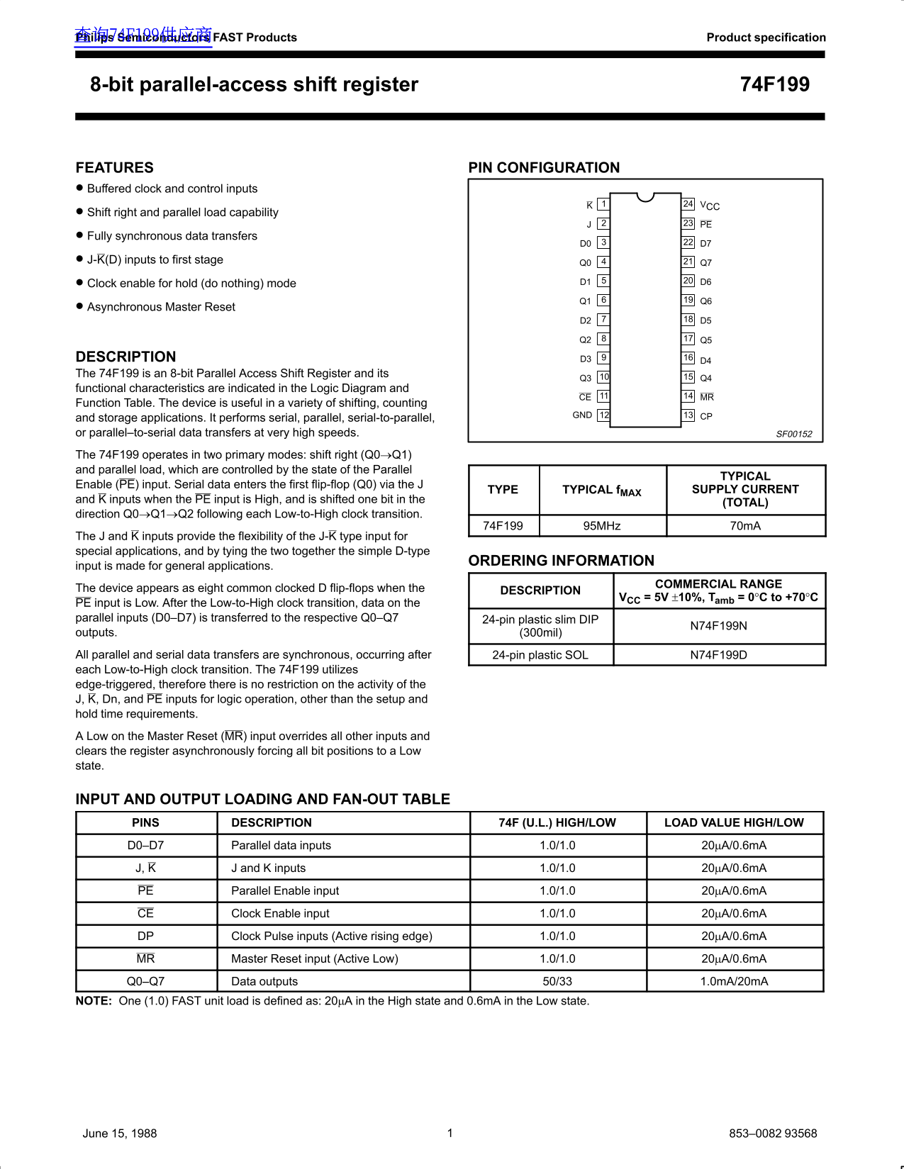
Page 1 Text Content
查询74F199供应商 Philips Semiconductors FAST Products Product specification
74F1998-bit parallel-access shift register
FEATURES PIN CONFIGURATION Buffered clock and control inputs
24K VCC
Shift right and parallel load capability
Fully synchronous data transfers
J-K(D) inputs to first stage Q0 Q7
Clock enable for hold (do nothing) mode D1 D6 Q1 Q6
Asynchronous Master Reset
DESCRIPTION D3 D4 The 74F199 is an 8-bit Parallel Access Shift Register and its
functional characteristics are indicated in the Logic Diagram and
CE MR
Function Table. The device is useful in a variety of shifting, counting
and storage applications. It performs serial, parallel, serial-to-parallel, CPGND
or parallel–to-serial data transfers at very high speeds. SF00152
The 74F199 operates in two primary modes: shift right (Q0→Q1) and parallel load, which are controlled by the state of the Parallel
TYPICAL
Enable (PE) input. Serial data enters the first flip-flop (Q0) via the J
TYPE TYPICAL f MAX SUPPLY CURRENT
and K inputs when the PE input is High, and is shifted one bit in the
(TOTAL)
direction Q0→Q1→Q2 following each Low-to-High clock transition.
74F199 95MHz 70m A
The J and K inputs provide the flexibility of the J-K type input for special applications, and by tying the two together the simple D-type
ORDERING INFORMATION
input is made for general applications.
COMMERCIAL RANGE
The device appears as eight common clocked D flip-flops when the DESCRIPTION
VCC = 5V ±10%, Tamb = 0°C to +70°C
PE input is Low. After the Low-to-High clock transition, data on the parallel inputs (D0–D7) is transferred to the respective Q0–Q7 24-pin plastic slim DIP
outputs. (300mil) All parallel and serial data transfers are synchronous, occurring after 24-pin plastic SOL N74F199D each Low-to-High clock transition. The 74F199 utilizes edge-triggered, therefore there is no restriction on the activity of the J, K, Dn, and PE inputs for logic operation, other than the setup and hold time requirements. A Low on the Master Reset (MR) input overrides all other inputs and clears the register asynchronously forcing all bit positions to a Low state.
INPUT AND OUTPUT LOADING AND FAN-OUT TABLE PINS DESCRIPTION 74F (U.L.) HIGH/LOW LOAD VALUE HIGH/LOW
D0–D7 Parallel data inputs 1.0/1.0 20µA/0.6m A J, K J and K inputs 1.0/1.0 20µA/0.6m A PE Parallel Enable input 1.0/1.0 20µA/0.6m A CE Clock Enable input 1.0/1.0 20µA/0.6m A DP Clock Pulse inputs (Active rising edge) 1.0/1.0 20µA/0.6m A MR Master Reset input (Active Low) 1.0/1.0 20µA/0.6m A Q0–Q7 Data outputs 50/33 1.0m A/20m A
NOTE: One (1.0) FAST unit load is defined as: 20µA in the High state and 0.6m A in the Low state.
1June 15, 1988 853–0082 93568
Page Summary Contents For Philips Semiconductors 8-bit Parallel-Access Shift Register 74F199 User Manual and Technical Specifications
Manual Details
| Brand | Philips |
|---|---|
| Pages | 8 |
| File Size | 66.09 KB |
| Published | July 07, 2026 |
Enter the captcha to get the download link:

Frequently Asked Questions
How do I asynchronously clear the register?
A Low on the Master Reset (MR) input overrides all other inputs and clears the register asynchronously.
What are the primary operational modes of the 74F199?
It operates in shift right ($ ext{Q0} ightarrow ext{Q1}$) and parallel load, controlled by the Parallel Enable (PE) input.
Can this device process data at high speeds?
Yes, it performs serial, parallel, serial-to-parallel, or parallel–to-serial data transfers at very high speeds.
What is required for all data transfers to occur?
All parallel and serial data transfers are synchronous, occurring after each Low-to-High clock transition (CP).