Page 1
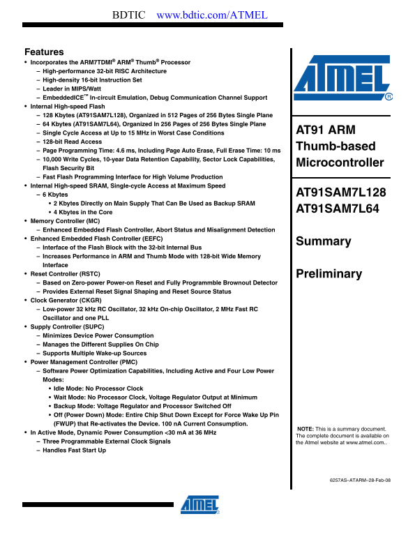
BDTIC www.bdtic.com/ATMEL Features Incorporates the ARM7TDMI® ARM® Thumb® Processor High-performance 32-bit RISC Architecture High-density 16-bit Instruction Set Leader in MIPS/Watt Embedded ICE™ In-c...
Page 2
Advanced Interrupt Controller (AIC) Individually Maskable, Eight-level Priority, Vectored Interrupt Sources Two External Interrupt Sources and One Fast Interrupt Source, Spurious Interrupt Protected D...
Page 3
AT91SAM7L128/64 Preliminary 1. Description The AT91SAM7L128/64 are low power members of Atmel’s Smart ARM Microcontroller family based on the 32-bit ARM7™ RISC processor and high-speed Flash memory. A...
Page 4
2. Block Diagram Figure 2-1. AT91SAM7L128/64 Block Diagram CAPP1 TDI CAPM1 TDO ICEJTAG Charge CAPP2 ARM7TDMI TMS Pump CAPM2 TCK SCAN Processor VDDINLCD JTAGSEL VDD3V6 LCD VDDLCD System Controller Volt...
Page 5
AT91SAM7L128/64 Preliminary 3. Signal Description Table 3-1. Signal Description List Active Voltage Signal Name Function Type Level Reference Comments Power I/O Lines (PIOC) and Voltage Regulator VDDI...
Page 6
Table 3-1. Signal Description List (Continued) Active Voltage Signal Name Function Type Level Reference Comments Reset/Test NRST Microcontroller Reset I/O Low VDDIO1 Internal Pull-up (100 kΩ) resistor...
Page 7
AT91SAM7L128/64 Preliminary Table 3-1. Signal Description List (Continued) Active Voltage Signal Name Function Type Level Reference Comments Two-Wire Interface TWD Two-wire Serial Data I/O TWCK Two-wi...
Page 8
4. Package and Pinout The AT91SAM7L128/64 is available in: 20 x 14 mm 128-lead LQFP package with a 0.5 mm lead-pitch 10 x 10 mm 144-ball LFBGA package with a 0.8 mm pitch. The part is also available i...
Page 9
AT91SAM7L128/64 Preliminary 4.2 128-lead LQFP Package Pinout Table 4-1. Pinout for 128-lead LQFP Package TST VDDLCD PB21 PC10/PGMM3 VDDCORE VDD3V6 PB22 PC11/PGMD0 PA0 CAPM2 PB23 PC12/PGMD1 PA1 CAPP2 G...
Page 10
4.3 144-ball LFBGA Package Outline Figure 4-2 shows the orientation of the 144-ball LFBGA package. A detailed mechanical description is given in the Mechanical Characteristics section of the prod- uct...
Page 11
AT91SAM7L128/64 Preliminary 4.4 144-ball LFBGA Pinout Table 4-2. SAM7L128/64 Pinout for 144-ball LFBGA Package Pin Signal Name Pin Signal Name Pin Signal Name Pin Signal Name A1 XOUT D1 PA6 G1 VDD3V6 ...
Page 12
5. Power Considerations 5.1 Power Supplies The AT91SAM7L128/64 has six types of power supply pins and integrates a voltage regulator, allowing the device to be supplied with only one voltage. The six ...
Page 13
AT91SAM7L128/64 Preliminary Table 5-1 on page 13 shows an example of backup mode with backup SRAM and RTC running. When entering this mode, all PIO pins keep their previous states, they are reinitiali...
Page 14
5.3 Wake-up Sources The wake-up events allow the device to exit from backup mode. When a wake-up event is detected, the supply controller performs a sequence which automatically reenables the voltage ...
Page 15
AT91SAM7L128/64 Preliminary Figure 5-2. Fast Start-Up Circuitry FSTT0 WKUP0 FSTT1 fast_restart WKUP1 FSTT15 WKUP15 5.5 Voltage Regulator The AT91SAM7L128/64 embeds a voltage regulator that is managed ...
Page 16
Adequate input supply decoupling is mandatory for VDDIO1 in order to improve startup stability and reduce source voltage drop. The input decoupling capacitor should be placed close to the chip. For ex...
Page 17
AT91SAM7L128/64 Preliminary Figure 5-4. The LCD Regulator is Externally Supplied VDDIO2 LCD Voltage Regulator External supply VDDLCD CAPP1 VDD3V6 CAPM1 Charge Pump CAPP2 VDDINLCD CAPM2 If the charge p...
Page 18
5.7 Typical Powering Schematics The AT91SAM7L128/64 supports a 1.8V-3.6V single supply mode. The internal regulator input connected to the source and its output feeds VDDCORE. Figure 5-6 shows the pow...
Page 19
AT91SAM7L128/64 Preliminary 6. I/O Line Considerations 6.1 JTAG Port Pins TMS, TDI and TCK are schmitt trigger inputs. TMS, TDI and TCK do not integrate a pull-up resistor. TDO is an output, driven at...
Page 20
6.6 PIO Controller Lines All the I/O lines; PA0 to PA25, PB0 to PB23, PC0 to PC29 integrate a programmable pull-up resistor. Programming of this pull-up resistor is performed independently for each I/...
Page 21
AT91SAM7L128/64 Preliminary 7. Processor and Architecture 7.1 ARM7TDMI Processor RISC processor based on ARMv4T Von Neumann Architecture Runs at up to 36 MHz, providing 0.9 MIPS/MHz Two instruction se...
Page 22
Embedded Flash interface, up to three programmable wait states Prefetch buffer, buffering and anticipating the 16-bit requests, reducing the required wait states Key-protected program, erase and lock/...
Page 23
AT91SAM7L128/64 Preliminary 8. Memories 128 Kbytes of Flash Memory (AT91SAM7L128) Single plane One bank of 512 pages of 256 bytes Fast access time, 15 MHz single-cycle access in Worst Case conditions ...
Page 24
Figure 8-1. Memory Mapping Internal Memory Mapping Note: (1) Can be ROM, Flash or SRAM Boot Memory (1) depending on GPNVM1 and REMAP 1 MBytes Flash before Remap SRAM after Remap 0x000F FFFF 0x0010 000...
Page 25
AT91SAM7L128/64 Preliminary 8.1 Embedded Memories 8.1.1 Internal Memories 8.1.1.1 Internal SRAM The AT91SAM7L128/64 embeds a high-speed 4-Kbyte SRAM bank and a 2-Kbyte backup SRAM bank. The backup SRA...
Page 26
Figure 8-2. Internal Memory Mapping with GPNVM Bit 1 = 0 (default) ROM Before Remap 1 Mbyte 0x000F FFFF Core SRAM (4 Kbytes) After Remap Internal FLASH 1 Mbyte 0x001F FFFF 0x0020 0000 Internal SRAM (C...
Page 27
AT91SAM7L128/64 Preliminary 8.1.2.3 Enhanced Embedded Flash Controller The Enhanced Embedded Flash Controller (EEFC) manages accesses performed by the mas- ters of the system. It enables reading the F...
Page 28
8.1.2.7 GPNVM Bits The AT91SAM7L128/64 features two GPNVM bits that can be cleared or set respectively through the commands “Clear GPNVM Bit” and “Set GPNVM Bit” of the EEFC User Interface.. Table 8-1...
Page 29
AT91SAM7L128/64 Preliminary 9. System Controller The System Controller manages all vital blocks of the microcontroller, interrupts, clocks, power, time, debug and reset. The System Controller Block Di...
Page 30
Figure 9-1. System Controller Block Diagram VDDIO1 vr_on Software Controlled VDDOUT vr_mode Voltage Regulator vr_ok supply_on Supply Controller CAPM1-CAPP1 NRSTB lcd_mode LCD Zero-Power Charge CAPM2-C...
Page 31
AT91SAM7L128/64 Preliminary 9.2 Supply Controller (SUPC) The Supply Controller controls the power supplies of each section of the product: the processor and the peripherals the Flash memory the backup...
Page 32
BOD current consumption is 25 µA, typically. To decrease current consumption, the software can disable the brownout detector, especially in low-power mode. The software can also configure the BOD in “...
Page 33
AT91SAM7L128/64 Preliminary Figure 9-2. Clock Generator Block Diagram Clock Generator MCK_SEL CLKIN Main Clock MAINCK Embedded 2 MHz RC Oscillator OSCSEL Embedded 32 k Hz RC Oscillator Slow Clock SLCK...
Page 34
Figure 9-3. Power Management Controller Block Diagram PCKProcessor Clock Controller Master Clock Controller Idle Mode MAINCK Prescaler PLLCK /1,/2,/4,...,/64 Peripherals periph_clk[2..14] Clock Contro...
Page 35
AT91SAM7L128/64 Preliminary One set of Chip ID Registers One Interface providing ICE Access Prevention Two-pin UART USART-compatible User Interface Programmable Baud Rate Generator Parity, Framing and...
Page 36
10. Peripherals 10.1 User Interface The User Peripherals are mapped in the 256 MBytes of the address space between 0x F000 0000 and 0x FFFF EFFF. Each peripheral is allocated 16 Kbytes of address spac...
Page 37
AT91SAM7L128/64 Preliminary 10.3 Peripheral Multiplexing on PIO Lines The AT91SAM7L128/64 features three PIO controllers, PIOA, PIOB and PIOC, that multiplex the I/O lines of the peripheral set. PIO C...
Page 38
10.4 PIO Controller A Multiplexing Table 10-2. Multiplexing on PIO Controller A PIO Controller A Application Usage I/O Line Peripheral A Peripheral B Extra Function Function Comments PA0 COM0 PA1 COM1...
Page 39
AT91SAM7L128/64 Preliminary 10.5 PIO Controller B Multiplexing Table 10-3. Multiplexing on PIO Controller B PIO Controller B Application Usage I/O Line Peripheral A Peripheral B Extra Function Functio...
Page 40
10.6 PIO Controller C Multiplexing Table 10-4. Multiplexing on PIO Controller C PIO Controller C Application Usage I/O Line Peripheral A Peripheral B Extra Functions Function Comments PC0 CTS1 PWM2 PG...