ADG936 Wideband 4 GHz, 36 dB Isolation at 1 GHz, CMOS 1.65 V to 2.75 V, Dual SPDT ADG936 ADG936- R User's Manual and Specifications Sheet
Summary
Discover the ADG936/ADG936-R wideband dual SPDT analog switches, precision components engineered for high-frequency wireless and RF communications. These switches feature low insertion loss and superior isolation, making them ideal for advanced digital transceiver front ends and feeder systems. This technical manual serves as a comprehensive guide, detailing performance specifications, operational modes (absorptive/reflective), optimal filtering selection, and advanced applications like antenna diversity switching for RF engineers and embedded designers building next-generation communication equipment.
Page 1 Text Content
查询ADG936BCP-500RL7供应商
Wideband 4 GHz, 36 d B Isolation at 1 GHz, FF IS LA TI (d
CMOS 1.65 V to 2.75 V, Dual SPDT
ADG936/ADG936-R FEATURES FUNCTIONAL BLOCK DIAGRAMS Wideband switch: −3 d B @ 4 GHz
RF1A RF1A
ADG936 absorptive dual SPDT ADG936-R reflective dual SPDT RFCA RFCA
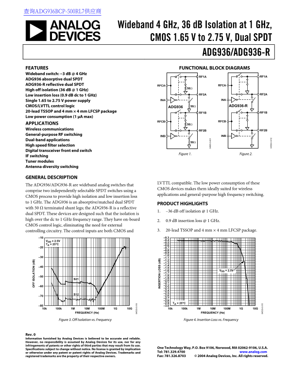
High off isolation (36 d B @ 1 GHz)
RF2A RF2A
Low insertion loss (0.9 d B dc to 1 GHz)
Single 1.65 to 2.75 V power supply INA INA CMOS/LVTTL control logic 50Ω ADG936-R
ADG936
20-lead TSSOP and 4 mm × 4 mm LFCSP package RF1B
Low power consumption (1 µA max)
RFCB RFCB
APPLICATIONS 50Ω Wireless communications RF2B
General-purpose RF switching
3- 0- INB INB
Dual-band applications
High speed filter selection Digital transceiver front end switch
Figure 1. Figure 2.
IF switching
IN SE TI SS (d
Tuner modules Antenna diversity switching
GENERAL DESCRIPTION
LVTTL compatible. The low power consumption of these
The ADG936/ADG936-R are wideband analog switches that
CMOS devices makes them ideally suited for wireless
comprise two independently selectable SPDT switches using a
applications and general-purpose high frequency switching.
CMOS process to provide high isolation and low insertion loss to 1 GHz. The ADG936 is an absorptive/matched dual SPDT
PRODUCT HIGHLIGHTS
with 50 Ω terminated shunt legs; the ADG936-R is a reflective
1. –36 d B off isolation @ 1 GHz. 3- 0-
dual SPDT. These devices are designed such that the isolation is high over the dc to 1 GHz frequency range. They have on-board
2. 0.9 d B insertion loss @ 1 GHz.
CMOS control logic, eliminating the need for external
controlling circuitry. The control inputs are both CMOS and 3. 20-lead TSSOP and 4 mm × 4 mm LFCSP package.
VDD = 2.5V –0.4 –0.5
TA = 25°C –0.6 –20 –0.7
–1.5 –1.6 VDD = 2.5V
–70 –2.6 –2.7 –2.8 –2.9 TA = 25°C –80 –3.0
FREQUENCY (Hz) FREQUENCY (Hz)
Figure 3. Off Isolation vs. Frequency Figure 4. Insertion Loss vs. Frequency
Rev. 0 Information furnished by Analog Devices is believed to be accurate and reliable. However, no responsibility is assumed by Analog Devices for its use, nor for any infringements of patents or other rights of third parties that may result from its use.
One Technology Way, P.O. Box 9106, Norwood, MA 02062-9106, U.S.A.
Specifications subject to change without notice. No license is granted by implication
or otherwise under any patent or patent rights of Analog Devices. Trademarks and Tel: 781.329.4700 www.analog.com registered trademarks are the property of their respective owners. Fax: 781.326.8703 © 2004 Analog Devices, Inc. All rights reserved.
Page Summary Contents For ADG936 Wideband 4 GHz, 36 dB Isolation at 1 GHz, CMOS 1.65 V to 2.75 V, Dual SPDT ADG936 ADG936- R User's Manual and Specifications Sheet
Manual Details
| Brand | Dual |
|---|---|
| Pages | 16 |
| File Size | 270.89 KB |
| Published | June 01, 2026 |
Enter the captcha to get the download link:

Frequently Asked Questions
What is the high off isolation at 1 GHz?
It provides a high isolation of 36 dB @ 1 GHz.
Is this switch compatible with CMOS control logic?
Yes, it features CMOS/LVTTL control logic, eliminating the need for external controlling circuitry.
What power supply voltage range must I use?
The unit requires a single power supply between 1.65 V and 2.75 V.
How does the ADG936 differ from the ADG936-R?
The ADG936 is an absorptive dual SPDT, while the ADG936-R is a reflective dual SPDT.