# A B C D E F G H I J K L M N O P Q R S T U V W X Y Z

AD7478 Analog Devices Data Sheet manual specifications

Summary

Discover the AD7476/AD7477/AD7478 series—highly efficient 12-, 10-, and 8-bit Successive Approximation Registered ADCs, designed for compact SOT-23 packages. These high-throughput, low-power devices are perfect for demanding applications such as medical instruments, battery-powered systems, and data acquisition hardware. This manual provides comprehensive technical details, including functional block diagrams, operational theory, detailed specifications, and application guidance necessary for seamless integration into your design.
📄 Preview 📖 Table of Contents Contents PAGE OF 24

Page 1 Text Content

1 MSPS, 12-/10-/8-Bit ADCs in 6-Lead SOT-23

AD7476/AD7477/AD7478

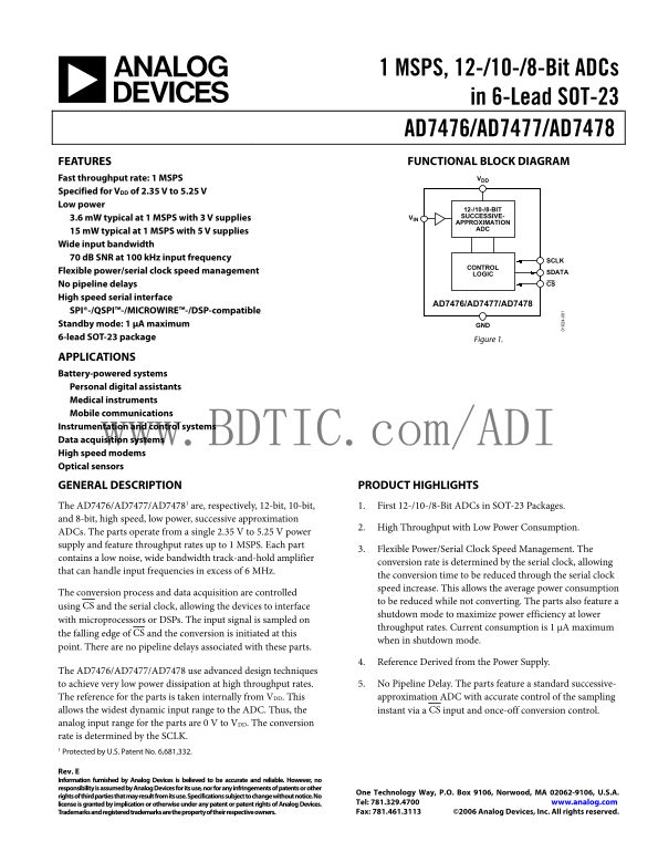
FEATURES FUNCTIONAL BLOCK DIAGRAM

Fast throughput rate: 1 MSPS VDD

Specified for VDD of 2.35 V to 5.25 V Low power

12-/10-/8-BIT VIN SUCCESSIVE-

3.6 m W typical at 1 MSPS with 3 V supplies

APPROXIMATION ADC

15 m W typical at 1 MSPS with 5 V supplies Wide input bandwidth 70 d B SNR at 100 k Hz input frequency

CONTROL

Flexible power/serial clock speed management SDATA

LOGIC

No pipeline delays CS

High speed serial interface

AD7476/AD7477/AD7478

SPI®-/QSPI™-/MICROWIRE™-/DSP-compatible Standby mode: 1 μA maximum GND 6-lead SOT-23 package Figure 1.

APPLICATIONS Battery-powered systems Personal digital assistants Medical instruments Mobile communications Instrumentation and control systems Data acquisition systems www.BDTIC.com/ADI High speed modems Optical sensors GENERAL DESCRIPTION PRODUCT HIGHLIGHTS The AD7476/AD7477/AD74781 are, respectively, 12-bit, 10-bit, 1. First 12-/10-/8-Bit ADCs in SOT-23 Packages. and 8-bit, high speed, low power, successive approximation

2. High Throughput with Low Power Consumption.

ADCs. The parts operate from a single 2.35 V to 5.25 V power supply and feature throughput rates up to 1 MSPS. Each part

3. Flexible Power/Serial Clock Speed Management. The

contains a low noise, wide bandwidth track-and-hold amplifier

conversion rate is determined by the serial clock, allowing 4-

that can handle input frequencies in excess of 6 MHz.

the conversion time to be reduced through the serial clock speed increase. This allows the average power consumption

The conversion process and data acquisition are controlled

to be reduced while not converting. The parts also feature a

using CS and the serial clock, allowing the devices to interface

shutdown mode to maximize power efficiency at lower

with microprocessors or DSPs. The input signal is sampled on

throughput rates. Current consumption is 1 μA maximum

the falling edge of CS and the conversion is initiated at this

when in shutdown mode.

point. There are no pipeline delays associated with these parts.

4. Reference Derived from the Power Supply.

The AD7476/AD7477/AD7478 use advanced design techniques

to achieve very low power dissipation at high throughput rates. 5. No Pipeline Delay. The parts feature a standard successive- The reference for the parts is taken internally from VDD. This approximation ADC with accurate control of the sampling

allows the widest dynamic input range to the ADC. Thus, the instant via a CS input and once-off conversion control. analog input range for the parts are 0 V to VDD. The conversion rate is determined by the SCLK. 1 Protected by U.S. Patent No. 6,681,332.

Rev. E Information furnished by Analog Devices is believed to be accurate and reliable. However, no responsibility is assumed by Analog Devices for its use, nor for any infringements of patents or other

One Technology Way, P.O. Box 9106, Norwood, MA 02062-9106, U.S.A.

rights of third parties that may result from its use. Specifications subject to change without notice. No

license is granted by implication or otherwise under any patent or patent rights of Analog Devices. Tel: 781.329.4700 www.analog.com Trademarks and registered trademarks are the property of their respective owners. Fax: 781.461.3113 ©2006 Analog Devices, Inc. All rights reserved.

Page Summary Contents For AD7478 Analog Devices Data Sheet manual specifications

Page 1 1 MSPS, 12-/10-/8-Bit ADCs in 6-Lead SOT-23 AD7476/AD7477/AD7478 FEATURES FUNCTIONAL BLOCK DIAGRAM Fast throughput rate: 1 MSPS VDD Specified for VDD of 2.35 V to 5.25 V Low power 12-/10-/8-BIT VIN SU...
Page 2 AD7476/AD7477/AD7478 TABLE OF CONTENTS Features Typical Performance Characteristics Applications....................................................................................... Terminology Func...
Page 3 AD7476/AD7477/AD7478 SPECIFICATIONS AD7476 SPECIFICATIONS A version: VDD = 2.7 V to 5.25 V, f SCLK = 20 MHz, f SAMPLE = 1 MSPS, unless otherwise noted; S and B versions: VDD = 2.35 V to 5.25 V, f SCLK...
Page 4 AD7476/AD7477/AD7478 Parameter A Version1,2 B Version1,2 S Version1,2 Unit Test Conditions/Comments LOGIC OUTPUT Output High Voltage, VOH VDD − 0.2 VDD − 0.2 VDD − 0.2 V min ISOURCE = 200 μA; VDD = 2....
Page 5 AD7476/AD7477/AD7478 AD7477 SPECIFICATIONS VDD = 2.7 V to 5.25 V, f SCLK = 20 MHz, TA = TMIN to TMAX, unless otherwise noted. Table 2. Parameter A Version1 S Version1,2 Unit Test Conditions/Comments D...
Page 6 AD7476/AD7477/AD7478 Parameter A Version1 S Version1,2 Unit Test Conditions/Comments POWER REQUIREMENTS VDD 2.7/5.25 2.7/5.25 V min/max IDD Digital I/Ps = 0 V or VDD Normal Mode (Static) 2 2 m A typ V...
Page 7 AD7476/AD7477/AD7478 AD7478 SPECIFICATIONS VDD = 2.7 V to 5.25 V, f SCLK = 20 MHz, TA = TMIN to TMAX, unless otherwise noted. Table 3. Parameter A Version1,2 S Version1,2 Unit Test Conditions/Comments...
Page 8 AD7476/AD7477/AD7478 Parameter A Version1,2 S Version1,2 Unit Test Conditions/Comments Power Dissipation5 Normal Mode (Operational) 17.5 17.5 m W max VDD = 5 V, f SAMPLE = 1 MSPS 4.8 4.8 m W max VDD =...
Page 9 AD7476/AD7477/AD7478 ABSOLUTE MAXIMUM RATINGS TA = 25°C, unless otherwise noted. Table 5. Parameter Rating Stresses above those listed under Absolute Maximum Ratings VDD to GND −0.3 V to +7 V may caus...
Page 10 AD7476/AD7477/AD7478 PIN CONFIGURATION AND FUNCTION DESCRIPTIONS 1VDD CS AD7476/ AD7477/ 2GND SDATA AD7478 TOP VIEW 3VIN SCLK (Not to Scale) Figure 3. Pin Configuration Table 6. Pin Function Descripti...
Page 11 AD7476/AD7477/AD7478 SN (d SN (d SN (d TYPICAL PERFORMANCE CHARACTERISTICS 8192 POINT FFT 8192 POINT FFT f SAMPLE = 1MSPS –10 f SAMPLE = 1MSPS f IN = 100k Hz f IN = 100k Hz SINAD = 71.67d B SINAD = 49...
Page 12 AD7476/AD7477/AD7478 Thus, for a 12-bit converter, this is 74 d B; for a 10-bit converter TERMINOLOGY it is 62 d B; and for an 8-bit converter it is 50 d B. Integral Nonlinearity Total Unadjusted Erro...
Page 13 AD7476/AD7477/AD7478 THEORY OF OPERATION CHARGE REDISTRIBUTION DAC CIRCUIT INFORMATION SAMPLING The AD7476/AD7477/AD7478 are, respectively, 12-bit, 10-bit, CAPACITOR COMPARATOR and 8-bit, fast, microp...
Page 14 AD7476/AD7477/AD7478 TYPICAL CONNECTION DIAGRAM Table 7. AD7476 SNR Performance Figure 14 shows a typical connection diagram for the Reference Tied to VDD 1 k Hz Input (d B) AD7476/AD7477/AD7478. VREF...
Page 15 AD7476/AD7477/AD7478 TH (d TH (d TH (d VDD = 2.7V Digital Input –10 f S = 605k SPS The digital input applied to the AD7476/AD7477/AD7478 is not limited by the maximum ratings that limit the analog inp...
Page 16 AD7476/AD7477/AD7478 Power-Down Mode If CS is brought high before the second SCLK falling edge, the This mode is intended for use in applications where slower part remains in normal mode and does not ...
Page 17 AD7476/AD7477/AD7478 This means that if the ADC powers up in the desired mode of Power-Up Time operation, and a dummy cycle is not required to change mode, The power-up time of the AD7476/AD7477/AD747...
Page 18 AD7476/AD7477/AD7478 SERIAL INTERFACE Sixteen serial clock cycles are required to perform the Figure 23, Figure 24, and Figure 25 show the detailed timing conversion process and to access data from th...
Page 19 AD7476/AD7477/AD7478 The frame synchronization signal generated on the TFS is tied MICROPROCESSOR INTERFACING to CS and, as with all signal processing applications, equidistant The serial interface on...
Page 20 AD7476/AD7477/AD7478 AD7476/ MC68HC161 AD7476/ DSP56xxx1 AD7477/ AD7477/ AD74781 AD74781 SCLK SCLK/PMC2 SCLK SCK MISO/PMC0SDATA SRDSDATA CS SS/PMC9 CS SC2 1ADDITIONAL PINS OMITTED FOR CLARITY 1ADDITIO...
Page 21 AD7476/AD7477/AD7478 OUTLINE DIMENSIONS 2.90 BSC 1.60 BSC 2.80 BSC PIN 1 INDICATOR 0.95 BSC 1.30 BSC 1.15 0.90 1.45 MAX 0.22 0.15 MAX 0.50 0.30 SEATING PLANE 0° 0.30 COMPLIANT TO JEDEC STANDARDS MO-17...
Page 22 AD7476/AD7477/AD7478 ORDERING GUIDE Model Temperature Range Linearity Error (LSB)1 Package Option2 Branding AD7476ART-500RL7 −40°C to +85°C ±1 typ RJ-6 CEA AD7476ART-REEL −40°C to +85°C ±1 typ RJ-6 CE...
Page 23 AD7476/AD7477/AD7478 NOTES www.BDTIC.com/ADI Rev. E | Page 23 of 24
Page 24 AD7476/AD7477/AD7478 NOTES www.BDTIC.com/ADI ©2006 Analog Devices, Inc. All rights reserved. Trademarks and registered trademarks are the property of their respective owners. C01024-0-4/06(E) Rev. E |...

Manual Details

Brand Analog Devices
Pages 24
File Size 512.38 KB
Published June 16, 2026
6 views

Enter the captcha to get the download link:

captcha

Frequently Asked Questions

What low power techniques do these ADCs use for efficiency?

They feature a shutdown mode with a maximum consumption of 1 μA, utilize flexible serial clock management, and optimize conversion time to reduce average power draw.

What types of interfaces or microprocessors are compatible with the AD747x series?

The devices support standard high-speed serialization using SPI®, QSPI™, MICROWIRE™, and are noted as being DSP-compatible.

How do I precisely control the analog input sampling process?

Data acquisition is controlled by signaling the CS, SCLK, and SDATA lines, allowing conversion initiation at the falling edge of the CS signal.

What are the maximum bandwidth capabilities for the input signal?

They feature a wide bandwidth track-and-hold amplifier that can handle input frequencies in excess of 6 MHz.