AD652 Analog Devices Data Manual/Specifications Sheet
Summary
This monolithic synchronous Voltage-to-Frequency Converter offers exceptional stability and ultra-low nonlinearity for precision analog signal processing. The manual provides comprehensive documentation on its operation, including multiple temperature grades (Commercial, Industrial, Extended), supply flexibility, and reliable integration guides. It is essential engineering hardware for developers building high-accuracy, stable systems that require predictable conversion performance in demanding environments, often meeting MIL-STD standards.
Page 1 Text Content
Monolithic Synchronous Voltage-to-Frequency Converter
AD652
FEATURES The AD652 is available in five performance grades. The 20-lead Full-scale frequency (up to 2 MHz) set by external system PLCC-packaged JP and KP grades are specified for operation clock over the 0°C to +70°C commercial temperature range. The
Extremely low linearity error (0.005% max at 1 MHz FS, 16-lead CERDIP-packaged AQ and BQ grades are specified for 0.02% max at 2 MHz FS) operation over the −40°C to +85°C industrial temperature No critical external components required
range. The AD652SQ is available for operation over the full
Accurate 5 V reference voltage
−55°C to +125°C extended temperature range.
Low drift (25 ppm/°C max)
Dual- or single-supply operation PRODUCT HIGHLIGHTS
Voltage or current input 1. The use of an external clock to set the full-scale frequency MIL-STD-883 compliant versions available allows the AD652 to achieve linearity and stability far
superior to other monolithic VFCs. By using the same clock
PRODUCT DESCRIPTION
to drive the AD652 and set the counting period (through a
The AD652 synchronous voltage-to-frequency converter
suitable divider), conversion accuracy is maintained
(SVFC) is a powerful building block for precision analog-to-
independent of variations in clock frequency.
digital conversion, offering typical nonlinearity of 0.002%
2. The AD652 synchronous VFC requires only one external
(0.005% maximum) at a 100 k Hz output frequency. The inher-
component (a noncritical integrator capacitor) for
ent monotonicity of the transfer function and wide range of
operation.
clock frequencies allow the conversion time and resolution to
be optimized for specific applications. 3. The AD652 includes a buffered, accurate 5 V reference. 4. The AD652’s clock input is TTL and CMOS compatible and
The AD652 uses a variation of the charge-balancing technique
can also be driven by sources referred to the negative power
to perform the conversion function. The AD652 uses an
supply. The flexible open-collector output stage provides
external clock to define the full-scale output frequency, rather
www.BDTIC.com/ADI
sufficient current sinking capability for TTL and CMOS
than relying on the stability of an external capacitor. The result
logic, as well as for optical couplers and pulse transformers.
is a more stable, more linear transfer function, with significant
A capacitor-programmable one-shot is provided for selec-
application benefits in both single- and multichannel systems.
tion of optimum output pulse width for power reduction.
Gain drift is minimized using a precision low drift reference
5. The AD652 can also be configured for use as a synchronous
and low TC, on-chip, thin-film scaling resistors. Furthermore,
F/V converter for isolated analog signal transmission.
initial gain error is reduced to less than 0.5% by the use of laser-
wafer-trimming. 6. The AD652 is available in versions compliant with MILSTD-883. Refer to the Analog Devices Military
The analog and digital sections of the AD652 have been
Products Databook or current AD652/883B data sheet for
designed to allow operation from a single-ended power source,
detailed specifications.
simplifying its use with isolated power supplies.
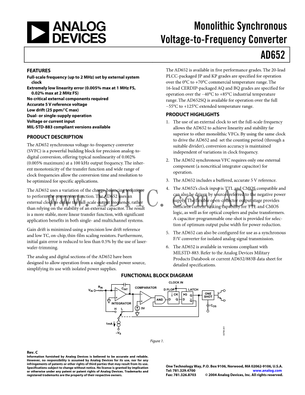
FUNCTIONAL BLOCK DIAGRAM
CLOCK IN
RIN COMPARATOR
VIN D FLOP LATCH
CK ONE SHOT
AND QD
INTEGRATOR
Figure 1.
Rev. C Information furnished by Analog Devices is believed to be accurate and reliable. However, no responsibility is assumed by Analog Devices for its use, nor for any infringements of patents or other rights of third parties that may result from its use.
One Technology Way, P.O. Box 9106, Norwood, MA 02062-9106, U.S.A.
Specifications subject to change without notice. No license is granted by implication
or otherwise under any patent or patent rights of Analog Devices. Trademarks and Tel: 781.329.4700 www.analog.com registered trademarks are the property of their respective owners. Fax: 781.326.8703 © 2004 Analog Devices, Inc. All rights reserved.
Page Summary Contents For AD652 Analog Devices Data Manual/Specifications Sheet
Manual Details
| Brand | Analog Devices |
|---|---|
| Pages | 28 |
| File Size | 637.70 KB |
| Published | June 05, 2026 |
Enter the captcha to get the download link:

Frequently Asked Questions
What temperature ranges are available for the AD652?
The device is available across grades supporting commercial (0°C to +70°C), industrial (-40°C to +85°C), and extended (-55°C to +125°C) use.
How does the AD652 maintain stable conversion accuracy?
It uses a single external clock source to simultaneously set both the full-scale frequency and the counting period, ensuring high linearity and stability.
What power supply configurations are supported by the VSC?
The AD652 supports dual or single-supply operations and can function with either voltage or current inputs.