SANYO ECH8315 Data Sheet
Summary
This manual provides comprehensive technical specifications and application details for the ECH8315 P-Channel Silicon MOSFET, an ideal general-purpose switching device. Featuring low ON-resistance and 4V drive capability, this semiconductor component is engineered for reliable power electronics applications. Designed for electrical engineers and hardware designers, the document covers absolute maximum ratings, detailed electrical characteristics, and usage considerations to ensure optimal integration and performance in various systems.
Page 1 Text Content
ECH8315
Ordering number : ENA1387
SANYO Semiconductors
DATA SHEET
P-Channel Silicon MOSFET
ECH8315 General-Purpose Switching Device Applications
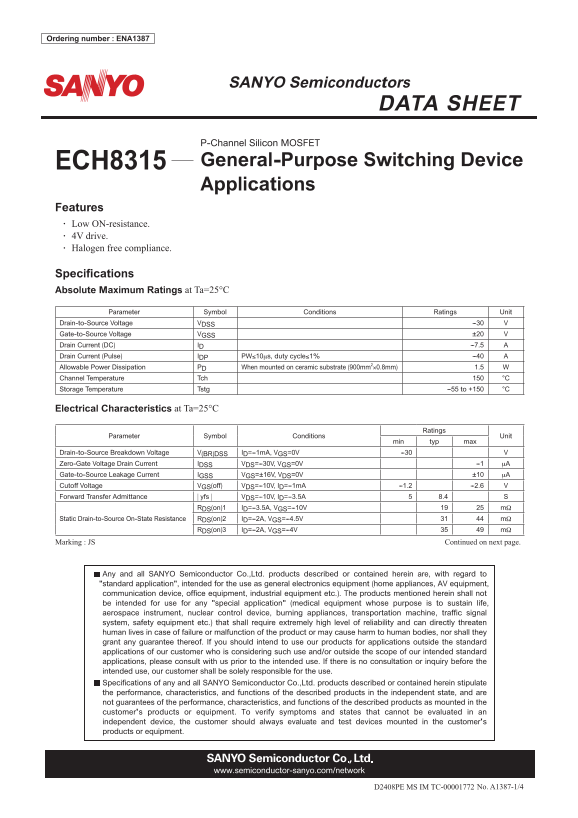
Features • Low ON-resistance. • 4V drive. • Halogen free compliance.
Specifi cations Absolute Maximum Ratings at Ta=25°C
Parameter Symbol Conditions Ratings Unit
Drain-to-Source Voltage VDSS --30 Gate-to-Source Voltage VGSS ±20 Drain Current (DC) ID --7.5 Drain Current (Pulse) IDP PW≤10μs, duty cycle≤1% --40
Allowable Power Dissipation PD When mounted on ceramic substrate (900mm2×0.8mm) 1.5
Channel Temperature Tch °C Storage Temperature Tstg --55 to +150 °C
Electrical Characteristics at Ta=25°C
Ratings
Parameter Symbol Conditions Unit
min typ max
Drain-to-Source Breakdown Voltage V(BR)DSS ID=--1m A, VGS=0V --30 Zero-Gate Voltage Drain Current IDSS VDS=--30V, VGS=0V --1 μA Gate-to-Source Leakage Current IGSS VGS=±16V, VDS=0V ±10 μA Cutoff Voltage VGS(off) VDS=--10V, ID=--1m A --1.2 --2.6 Forward Transfer Admittance | yfs | VDS=--10V, ID=--3.5A 8.4
RDS(on)1 ID=--3.5A, VGS=--10V mΩ Static Drain-to-Source On-State Resistance RDS(on)2 ID=--2A, VGS=--4.5V mΩ RDS(on)3 ID=--2A, VGS=--4V mΩ
Marking : JS Continued on next page.
Any and all SANYO Semiconductor Co.,Ltd. products described or contained herein are, with regard to "standard application", intended for the use as general electronics equipment (home appliances, AV equipment, communication device, office equipment, industrial equipment etc.). The products mentioned herein shall not be intended for use for any "special application" (medical equipment whose purpose is to sustain life, aerospace instrument, nuclear control device, burning appliances, transportation machine, traffic signal system, safety equipment etc.) that shall require extremely high level of reliability and can directly threaten human lives in case of failure or malfunction of the product or may cause harm to human bodies, nor shall they grant any guarantee thereof. If you should intend to use our products for applications outside the standard applications of our customer who is considering such use and/or outside the scope of our intended standard applications, please consult with us prior to the intended use. If there is no consultation or inquiry before the intended use, our customer shall be solely responsible for the use. Specifications of any and all SANYO Semiconductor Co.,Ltd. products described or contained herein stipulate the performance, characteristics, and functions of the described products in the independent state, and are not guarantees of the performance, characteristics, and functions of the described products as mounted in the customer's products or equipment. To verify symptoms and states that cannot be evaluated in an independent device, the customer should always evaluate and test devices mounted in the customer's products or equipment.
www.semiconductor-sanyo.com/network
D2408PE MS IM TC-00001772
No. A1387-1/4
Page Summary Contents For SANYO ECH8315 Data Sheet
Manual Details
| Brand | Sanyo |
|---|---|
| Pages | 4 |
| File Size | 275.29 KB |
| Published | June 04, 2026 |
Enter the captcha to get the download link:

Frequently Asked Questions
Can I use this MOSFET for life support or medical equipment?
No, this product is not intended for 'special application' that requires extreme reliability; consult Sanyo Semiconductors if you plan such usage.
What are the typical on-state resistance values?
The R(on)2 (static drain-to-source) typically ranges from 31 to 44 mΩ, depending on testing conditions and current applied.
What is the absolute maximum allowable power dissipation?
When mounted on a ceramic substrate (900mm 0.8mm), the allowed power dissipation P is rated at 1.5 W.