Optically Isolated Error Amplifier by Fairchild Semiconductor - Page 1 of 15
Summary
This integrated optocoupler and error amplifier solution simplifies the design of isolated power supplies. Combining a precision 2.5V reference, an error amplifier, and high-isolation optocoupling (up to 5000V), it is indispensable for creating compact, regulated AC/DC or DC/DC converters. The provided manual offers comprehensive technical documentation, including detailed electrical characteristics, application guides, and material specifications necessary for power supply designers seeking a high-precision component that minimizes required parts and enhances system reliability.
Page 1 Text Content
OPTICALLY ISOLATED ERROR AMPLIFIER
FOD2741A FOD2741B FOD2741C
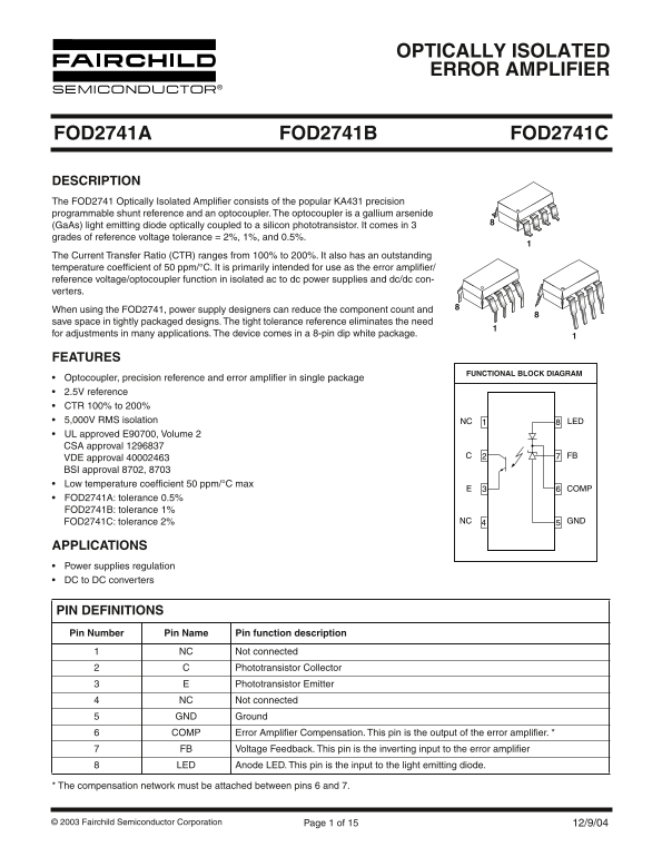
DESCRIPTION The FOD2741 Optically Isolated Amplifier consists of the popular KA431 precision programmable shunt reference and an optocoupler. The optocoupler is a gallium arsenide (Ga As) light emitting diode optically coupled to a silicon phototransistor. It comes in 3 grades of reference voltage tolerance = 2%, 1%, and 0.5%. The Current Transfer Ratio (CTR) ranges from 100% to 200%. It also has an outstanding temperature coefficient of 50 ppm/°C. It is primarily intended for use as the error amplifier/ reference voltage/optocoupler function in isolated ac to dc power supplies and dc/dc con- verters. When using the FOD2741, power supply designers can reduce the component count and save space in tightly packaged designs. The tight tolerance reference eliminates the need for adjustments in many applications. The device comes in a 8-pin dip white package.
FEATURES
FUNCTIONAL BLOCK DIAGRAM
Optocoupler, precision reference and error amplifier in single package 2.5V reference CTR 100% to 200% 5,000V RMS isolation NC LED UL approved E90700, Volume 2 CSA approval 1296837
VDE approval 40002463 BSI approval 8702, 8703 Low temperature coefficient 50 ppm/°C max
FOD2741A: tolerance 0.5% FOD2741B: tolerance 1%
FOD2741C: tolerance 2% NC GND
APPLICATIONS Power supplies regulation DC to DC converters
PIN DEFINITIONS Pin Number Pin Name Pin function description
NC Not connected
Phototransistor Collector Phototransistor Emitter
NC Not connected GND Ground COMP Error Amplifier Compensation. This pin is the output of the error amplifier. * FB Voltage Feedback. This pin is the inverting input to the error amplifier LED Anode LED. This pin is the input to the light emitting diode.
* The compensation network must be attached between pins 6 and 7.
© 2003 Fairchild Semiconductor Corporation Page 1 of 15 12/9/04
Page Summary Contents For Optically Isolated Error Amplifier by Fairchild Semiconductor - Page 1 of 15
Manual Details
| Brand | Fairchild |
|---|---|
| Pages | 16 |
| File Size | 191.90 KB |
| Published | May 30, 2026 |
Enter the captcha to get the download link:

Frequently Asked Questions
What determines which version of the device to use (A, B, or C)?
The variant determines the reference voltage tolerance: A is 0.5%, B is 1%, and C is 2%.
How should the compensation network be attached?
The compensation network must be attached between pin 6 (COMP - Error Amplifier) and pin 7 (FB - Voltage Feedback).
What level of isolation does this amplifier provide?
It provides an outstanding 5,000V RMS isolation in a single package.
What is the required operating temperature range for this device?
The specified operating temperature range is from -25°C to +85°C.