# A B C D E F G H I J K L M N O P Q R S T U V W X Y Z

National Semiconductor LP2987 LP2988 Micropower, 200 mA Ultra Low-Dropout Voltage User Manual

Summary

Discover the LP2987/LP2988 series, ultra-low-dropout LDO voltage regulators engineered for reliable power management in portable and noise-sensitive equipment. Ideal for applications like cellular phones, digital cameras, laptops, and complex electronics requiring stable output voltages (e.g., 3.3V, 5.0V). This resource provides comprehensive guidance on configuring and integrating the regulator, covering key features such as programmable power-on reset delay, ultra-low quiescent current draw, and noise reduction capabilities.
📄 Preview PAGE OF 19

Page 1 Text Content

查询LP2987供应商

LP 2987/LP icropow er,200 ltra Low -D ropout Voltage egulator ith rogram able ow er-O eset elay

March

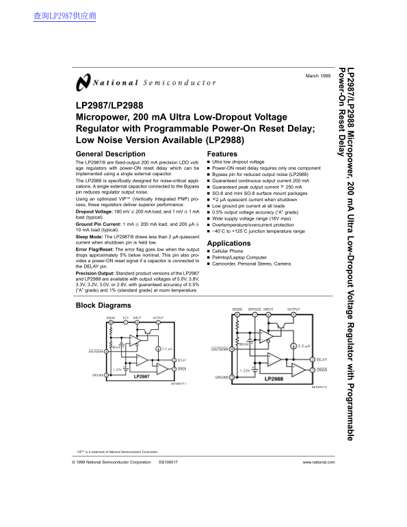
LP2987/LP2988 Micropower, m A Ultra Low-Dropout Voltage Regulator with Programmable Power-On Reset Delay; Low Noise Version Available (LP2988) General Description Features

The LP2987/8 are fixed-output m A precision LDO volt- Ultra low dropout voltage

age regulators with power-ON reset delay which can be Power-ON reset delay requires only one component implemented using single external capacitor. Bypass pin for reduced output noise (LP2988) The LP2988 is specifically designed for noise-critical appli- Guaranteed continuous output current m A cations. single external capacitor connected to the Bypass Guaranteed peak output current m A pin reduces regulator output noise.

SO-8 and mini SO-8 surface mount packages

Using an optimized VIP™ (Vertically Integrated PNP) pro- <2 µA quiescent current when shutdown cess, these regulators deliver superior performance: Low ground pin current at all loads Dropout Voltage: m V m A load, and m V m A 0.5% output voltage accuracy (“A” grade) load (typical). Wide supply voltage range (16V max) Ground Pin Current: m A m A load, and µA Overtemperature/overcurrent protection m A load (typical). −40˚C to +125˚C junction temperature range Sleep Mode: The LP2987/8 draws less than µA quiescent current when shutdown pin is held low. Applications Error Flag/Reset: The error flag goes low when the output

Cellular Phone

drops approximately 5% below nominal. This pin also pro-

Palmtop/Laptop Computer

vides power-ON reset signal if capacitor is connected to

Camcorder, Personal Stereo, Camera

the DELAY pin. Precision Output: Standard product versions of the LP2987 and LP2988 are available with output voltages of 5.0V, 3.8V, 3.3V, 3.2V, 3.0V, or 2.8V, with guaranteed accuracy of 0.5% (“A” grade) and 1% (standard grade) at room temperature.

Block Diagrams

DS100017-1

DS100017-2

VIP™ is trademark of National Semiconductor Corporation.

National Semiconductor Corporation DS100017 www.national.com

Page Summary Contents For National Semiconductor LP2987 LP2988 Micropower, 200 mA Ultra Low-Dropout Voltage User Manual

Page 1 查询LP2987供应商 LP 2987/LP icropow er,200 ltra Low -D ropout Voltage egulator ith rogram able ow er-O eset elay March LP2987/LP2988 Micropower, m A Ultra Low-Dropout Voltage Regulator with Programmable Po...
Page 2 Connection Diagram (LP2987) Surface Mount Packages: Mini SO-8 Package Type MM: See NS Package Drawing Number MUA08A SO-8 Package Type M: See NS Package Drawing Number M08A DS100017-3 For ordering info...
Page 3 Ordering Information (LP2987) (Continued) TABLE 1. Package Marking and Ordering Information (Continued) Output Voltage Grade Order Information Package Marking Supplied as: 3.3 STD LP2987IMX-3.3 2987IM...
Page 4 Connection Diagram (LP2988) Surface Mount Packages: Mini SO-8 Package Type MM: See NS Package Drawing Number MUA08A SO-8 Package Type M: See NS Package Drawing Number M08A DS100017-16 For ordering inf...
Page 5 Ordering Information (LP2988) (Continued) TABLE 2. Package Marking and Ordering Information (Continued) Output Voltage Grade Order Information Package Marking Supplied as: 3.3 STD LP2988IMX-3.3 2988IM...
Page 6 Absolute Maximum Ratings (Note 1) Input Supply Voltage (Operating) 2.1V to +16V If Military/Aerospace specified devices are required, please contact the National Semiconductor Sales Office/ Shutdown P...
Page 7 Electrical Characteristics (Continued) Limits in standard typeface are for TJ 25˚C, and limits in boldface type apply over the full operating temperature range. Un- less otherwise specified: VIN VO(NO...
Page 8 Typical Performance Characteristics Unless otherwise specified: TA 25˚C, COUT 4.7 µF, CIN 2.2 µF, S/D is tied to VIN, VIN VO(NOM) 1V, IL m A. VOUT vs Temperature Dropout Voltage vs Temperature DS10001...
Page 9 Typical Performance Characteristics Unless otherwise specified: TA 25˚C, COUT 4.7 µF, CIN 2.2 µF, S/D is tied to VIN, VIN VO(NOM) 1V, IL m A. (Continued) Input Current vs VIN Input Current vs VIN DS10...
Page 10 Typical Performance Characteristics Unless otherwise specified: TA 25˚C, COUT 4.7 µF, CIN 2.2 µF, S/D is tied to VIN, VIN VO(NOM) 1V, IL m A. (Continued) Turn-On Waveform Turn-On Waveform DS100017-30 ...
Page 11 Typical Performance Characteristics Unless otherwise specified: TA 25˚C, COUT 4.7 µF, CIN 2.2 µF, S/D is tied to VIN, VIN VO(NOM) 1V, IL m A. (Continued) Shutdown Pin Current vs DC Load Regulation Shu...
Page 12 Typical Performance Characteristics Unless otherwise specified: TA 25˚C, COUT 4.7 µF, CIN 2.2 µF, S/D is tied to VIN, VIN VO(NOM) 1V, IL m A. (Continued) Delay Sink Current vs Temperature Delay Sink C...
Page 13 Typical Performance Characteristics Unless otherwise specified: TA 25˚C, COUT 4.7 µF, CIN 2.2 µF, S/D is tied to VIN, VIN VO(NOM) 1V, IL m A. (Continued) Output Noise Voltage (LP2988) Output Noise Den...
Page 14 Typical Performance Characteristics Unless otherwise specified: TA 25˚C, COUT 4.7 µF, CIN 2.2 µF, S/D is tied to VIN, VIN VO(NOM) 1V, IL m A. (Continued) Turn-On Time (LP2988) DS100017-56 Basic Applic...
Page 15 quired amount of output capacitance is provided over the full Application Hints operating temperature range. good Tantalum capacitor will show very little variation with temperature, but ceramic EXTER...
Page 16 Application Hints (Continued) DS100017-9 Timing Diagram for Power-Up The external capacitor c DLY sets the delay time (TDELAY). The value of capacitor required for given time delay may be calculated u...
Page 17 Application Hints Care must be taken to ensure that the capacitor selected for (Continued) bypass will not have significant leakage current over the op- To assure proper operation, the signal source u...
Page 18 Physical Dimensions inches (millimeters) unless otherwise noted Mini SO-8 Package Type MM NS Package Number MUA08A www.national.com
Page 19 LP 2987/LP icropow er,200 ltra Low -D ropout Voltage egulator ith rogram able ow er-O eset elay Physical Dimensions inches (millimeters) unless otherwise noted (Continued) SO-8 Package Type NS Package...

Manual Details

Brand National
Pages 19
File Size 517.39 KB
Published June 06, 2026
51 views

Enter the captcha to get the download link:

captcha

Frequently Asked Questions

How do I implement the power-on reset delay?

It only requires a single external capacitor connected to the DELAY pin.

Which model is best for noise-critical applications?

The LP2988, which features a Bypass pin for reduced output noise, is specifically designed for these uses.

What are the operating temperature and protection limits?

The regulators support a junction temperature range of −40°C to +125°C and include overtemperature/overcurrent protection.

What standard output voltages can I order?

Available options include 5.0V, 3.8V, 3.3V, 3.2V, 3.0V, or 2.8V.