ANALOG DEVICES Voltage-to-Frequency and Frequency-to-Voltage Converter AD650 User Guide
Summary
The AD650 is a high-performance Voltage-to-Frequency, Frequency-to-Voltage, and V/F converter designed for precision signal processing up to 1 MHz. This manual provides comprehensive technical details, including functional block diagrams, application specifications across various packages (DIP, PLCC), and operational guidelines for challenging industrial temperature ranges. It is essential reading for electronics engineers and designers requiring high-linearity analog signal conversion in applications like motor control, demodulators, or precision measurement circuits.
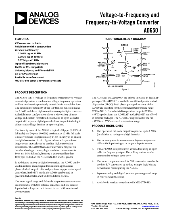
Page 1 Text Content
Voltage-to-Frequency and Frequency-to-Voltage Converter
AD650
FEATURES FUNCTIONAL BLOCK DIAGRAM
V/F conversion to 1 MHz
AD650
Reliable monolithic construction OFFSET
1VOUT
NULLINPUT
Very low nonlinearity OFFSET
AMP TRIM OFFSET
0.002% typ at 10 k Hz 2+IN
0.005% typ at 100 k Hz
3–IN +VS
0.07% typ at 1 MHz
BIPOLAR
Input offset trimmable to zero S1 ANALOG
OFFSET
CURRENT 1m A
CMOS- or TTL-compatible –VS –0.6V
DIGITAL
Unipolar, bipolar, or differential V/F OUT –VS GND
V/F or F/V conversion ONE FREQ ONE COMPARATOR SHOT OUT
SHOT INPUT
CAPACITOR COMP
Available in surface mount
MIL-STD-883 compliant versions available 7NC FOUTPUT
NC = NO CONNECT
Figure 1.
PRODUCT DESCRIPTION The AD650 V/F/V (voltage-to-frequency or frequency-to-voltage The AD650JN and AD650KN are offered in plastic 14-lead DIP converter) provides a combination of high frequency operation packages. The AD650JP is available in a 20-lead plastic leaded and low nonlinearity previously unavailable in monolithic form. chip carrier (PLCC). Both plastic packaged versions of the The inherent monotonicity of the V/F transfer function makes AD650 are specified for the commercial temperature range the AD650 useful as a high-resolution analog-to-digital converter. (0°C to 70°C). For industrial temperature range (−25°C to A flexible input configuration allows a wide variety of input +85°C) applications, the AD650AD and AD650BD are offered voltage and current formats to be used, and an open-collector in ceramic packages. The AD650SD is specified for the full
output with separate digital ground allows simple interfacing to −55°C to +125°C extended temperature range.
either standard logic families or opto-couplers.
PRODUCT HIGHLIGHTS
The linearity error of the AD650 is typically 20 ppm (0.002% of
1. Can operate at full-scale output frequencies up to 1 MHz
full scale) and 50 ppm (0.005%) maximum at 10 k Hz full scale.
(in addition to having very high linearity).
This corresponds to approximately 14-bit linearity in an analog-
to-digital converter circuit. Higher full-scale frequencies or 2. Can be configured to accommodate bipolar, unipolar, or longer count intervals can be used for higher resolution differential input voltages, or unipolar input currents.
conversions. The AD650 has a useful dynamic range of six
3. TTL or CMOS compatibility is achieved by using an open
decades allowing extremely high resolution measurements.
collector frequency output. The pull-up resistor can be
Even at 1 MHz full scale, linearity is guaranteed less than
connected to voltages up to 30 V.
1000 ppm (0.1%) on the AD650KN, BD, and SD grades.
4. The same components used for V/F conversion can also be
In addition to analog-to-digital conversion, the AD650 can be
used for F/V conversion by adding a simple logic biasing
used in isolated analog signal transmission applications,
network and reconfiguring the AD650.
phased-locked loop circuits, and precision stepper motor speed controllers. In the F/V mode, the AD650 can be used in
5. Separate analog and digital grounds prevent ground loops
precision tachometer and FM demodulator circuits.
in real-world applications.
The input signal range and full-scale output frequency are user-
6. Available in versions compliant with MIL-STD-883.
programmable with two external capacitors and one resistor. Input offset voltage can be trimmed to zero with an external potentiometer.
Rev. D Information furnished by Analog Devices is believed to be accurate and reliable. However, no responsibility is assumed by Analog Devices for its use, nor for any infringements of patents or other
One Technology Way, P.O. Box 9106, Norwood, MA 02062-9106, U.S.A.
rights of third parties that may result from its use. Specifications subject to change without notice. No
license is granted by implication or otherwise under any patent or patent rights of Analog Devices. Tel: 781.329.4700 www.analog.com Trademarks and registered trademarks are the property of their respective owners. Fax: 781.461.3113 ©2006 Analog Devices, Inc. All rights reserved.
Page Summary Contents For ANALOG DEVICES Voltage-to-Frequency and Frequency-to-Voltage Converter AD650 User Guide
Manual Details
| Brand | Analog Devices |
|---|---|
| Pages | 20 |
| File Size | 429.07 KB |
| Published | May 14, 2026 |
Enter the captcha to get the download link:

Frequently Asked Questions
What is the maximum operating temperature range for all AD650 versions?
The full-featured AD650SD grade supports an extended range of -55°C to +125°C.
How can I ensure high resolution and minimize ground loop issues when using the device?
Utilize separate analog and digital grounds, which prevents ground loops and simplifies interfacing.
Is the AD650 compatible with different logic circuits?
Yes, it achieves TTL or CMOS compatibility by using an open collector output, allowing connection to voltages up to 30 V.
What is the typical linearity error stated for the AD650 product generally?
The linearity error is typically 20 ppm (0.002% of full scale), corresponding to approximately 14-bit linearity.