# A B C D E F G H I J K L M N O P Q R S T U V W X Y Z

AD Analog Devices ADM1067 Data Sheet Manual

Summary

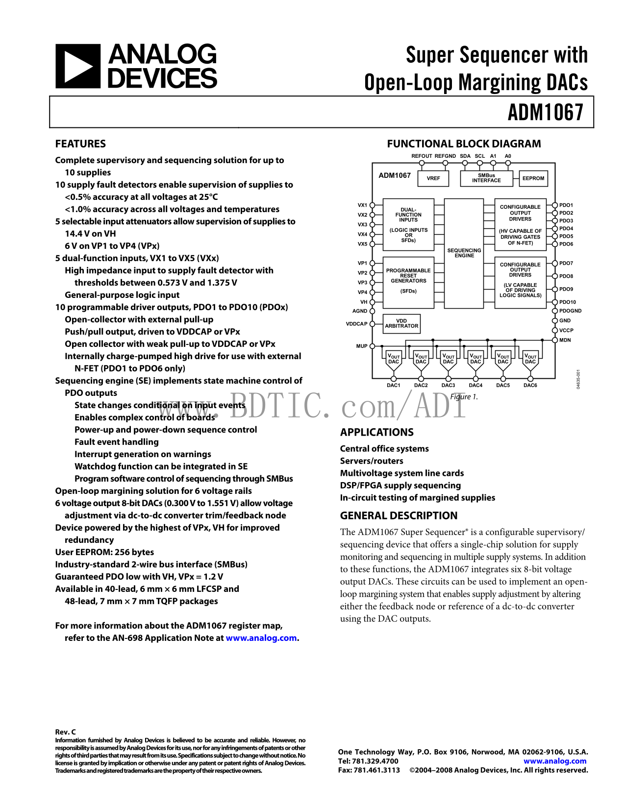
This configurable supervisory and sequencing device provides an advanced single-chip solution for monitoring and managing up to 10 power supplies. Featuring Open-Loop Margining DACs via an SMBus interface, it enables precise voltage adjustment and reliable fault detection across complex multi-voltage systems. The accompanying documentation guides engineers through implementation details, covering sophisticated sequence control, state machine logic, and optimal setup for high-reliability applications such as servers, routers, and central office equipment.
📄 Preview PAGE OF 32

Page 1 Text Content

Super Sequencer with Open-Loop Margining DACs

ADM1067 FEATURES FUNCTIONAL BLOCK DIAGRAM

REFOUT REFGND SDA SCL A1 A0

Complete supervisory and sequencing solution for up to 10 supplies SMBus

VREF EEPROMADM1067

INTERFACE

10 supply fault detectors enable supervision of supplies to <0.5% accuracy at all voltages at 25°C

VX1 CONFIGURABLE PDO1

<1.0% accuracy across all voltages and temperatures DUAL-

VX2 FUNCTION OUTPUT PDO2

INPUTS DRIVERS PDO3

5 selectable input attenuators allow supervision of supplies to VX3

(LOGIC INPUTS PDO4

(HV CAPABLE OF

14.4 V on VH VX4 OR PDO5

DRIVING GATES

SFDs)

VX5 OF N-FET) PDO6

6 V on VP1 to VP4 (VPx)

SEQUENCING ENGINE

5 dual-function inputs, VX1 to VX5 (VXx)

VP1 CONFIGURABLE PDO7

High impedance input to supply fault detector with PROGRAMMABLE OUTPUT

VP2 DRIVERS

RESET PDO8 VP3 GENERATORS

thresholds between 0.573 V and 1.375 V (LV CAPABLE

(SFDs) OF DRIVING PDO9

General-purpose logic input LOGIC SIGNALS)

VH PDO10

10 programmable driver outputs, PDO1 to PDO10 (PDOx)

AGND PDOGND

Open-collector with external pull-up VDD GND

ARBITRATORVDDCAP

Push/pull output, driven to VDDCAP or VPx

Open collector with weak pull-up to VDDCAP or VPx MUP

Internally charge-pumped high drive for use with external VOUT VOUT VOUT VOUT VOUT VOUT DAC DAC DAC DAC DAC DAC

N-FET (PDO1 to PDO6 only) Sequencing engine (SE) implements state machine control of

DAC1 DAC2 DAC3 DAC4 DAC5 DAC6

PDO outputs

Figure 1.

State changes conditional on input events

www.BDTIC.com/ADI Enables complex control of boards Power-up and power-down sequence control

APPLICATIONS

Fault event handling

Central office systems

Interrupt generation on warnings

Servers/routers

Watchdog function can be integrated in SE

Multivoltage system line cards

Program software control of sequencing through SMBus

DSP/FPGA supply sequencing

Open-loop margining solution for 6 voltage rails

In-circuit testing of margined supplies

6 voltage output 8-bit DACs (0.300 V to 1.551 V) allow voltage adjustment via dc-to-dc converter trim/feedback node GENERAL DESCRIPTION Device powered by the highest of VPx, VH for improved

The ADM1067 Super Sequencer® is a configurable supervisory/

redundancy

sequencing device that offers a single-chip solution for supply

User EEPROM: 256 bytes

monitoring and sequencing in multiple supply systems. In addition

Industry-standard 2-wire bus interface (SMBus)

to these functions, the ADM1067 integrates six 8-bit voltage

Guaranteed PDO low with VH, VPx = 1.2 V 5-

output DACs. These circuits can be used to implement an open-

Available in 40-lead, 6 mm × 6 mm LFCSP and

loop margining system that enables supply adjustment by altering

48-lead, 7 mm × 7 mm TQFP packages

either the feedback node or reference of a dc-to-dc converter using the DAC outputs.

For more information about the ADM1067 register map, refer to the AN-698 Application Note at www.analog.com.

Rev. C Information furnished by Analog Devices is believed to be accurate and reliable. However, no responsibility is assumed by Analog Devices for its use, nor for any infringements of patents or other

One Technology Way, P.O. Box 9106, Norwood, MA 02062-9106, U.S.A.

rights of third parties that may result from its use. Specifications subject to change without notice. No

license is granted by implication or otherwise under any patent or patent rights of Analog Devices. Tel: 781.329.4700 www.analog.com Trademarks and registered trademarks are the property of their respective owners. Fax: 781.461.3113 ©2004–2008 Analog Devices, Inc. All rights reserved.

Page Summary Contents For AD Analog Devices ADM1067 Data Sheet Manual

Page 1 Super Sequencer with Open-Loop Margining DACs ADM1067 FEATURES FUNCTIONAL BLOCK DIAGRAM REFOUT REFGND SDA SCL A1 A0 Complete supervisory and sequencing solution for up to 10 supplies SMBus VREF EEPROM...
Page 2 ADM1067 TABLE OF CONTENTS Features Warnings...................................................................................... Functional Block Diagram SMBus Jump (Unconditional Jump).................
Page 3 ADM1067 Six of these programmable outputs can also provide up to a 12 V Supply margining can be performed with a minimum of external output for driving the gate of an N-FET that can be placed in compo...
Page 4 ADM1067 SPECIFICATIONS VH = 3.0 V to 14.4 V1, VPx = 3.0 V to 6.0 V1, TA = −40°C to +85°C, unless otherwise noted. Table 1. Parameter Min Typ Max Unit Test Conditions/Comments POWER SUPPLY ARBITRATION ...
Page 5 ADM1067 Parameter Min Typ Max Unit Test Conditions/Comments INL ±0.75 LSB Endpoint corrected DNL ±0.4 LSB Gain Error 1 % Maximum Load Current (Source) 100 μA Maximum Load Current (Sink) 100 μA Maximum...
Page 6 ADM1067 Parameter Min Typ Max Unit Test Conditions/Comments SERIAL BUS TIMING Clock Frequency, f SCLK 400 k Hz Bus Free Time, t BUF 4.7 μs Start Setup Time, t SU;STA 4.7 μs Stop Setup Time, t SU;STO 4...
Page 7 ADM1067 ABSOLUTE MAXIMUM RATINGS Table 2. THERMAL RESISTANCE Parameter Rating Voltage on VH Pin 16 V θJA is specified for the worst-case conditions, that is, a device Voltage on VPx Pins 7 V soldered ...
Page 8 ADM1067 PIN CONFIGURATIONS AND FUNCTION DESCRIPTIONS EF VD NC NC36 PIN 1 SC VX1 INDICATOR PDO135 VX1 PDO130 VX2 PDO234 PIN 1 VX2 INDICATOR PDO229 VX3 PDO333 VX3 PDO328 VX4 PDO432 VC VX5 ADM1067 PDO531...
Page 9 ADM1067 Pin No. LFCSP1 TQFP Mnemonic Description 38 45 MDN Digital Input. Forces DACs to their highest value, causing the voltage at the feedback node to rise. This is compensated for by a decrease in...
Page 10 ADM1067 P1 (m (V (V TYPICAL PERFORMANCE CHARACTERISTICS VVP1 (V) VVP1 (V) Figure 5. VVDDCAP vs. VVP1 Figure 8. IVP1 vs. VVP1 (VP1 Not as Supply) www.BDTIC.com/ADI VVH (V) VVH (V) Figure 9. IVH vs. VVH...
Page 11 ADM1067 (V (V E- PU PE (V DAC 20kΩ BUFFER PROBE OUTPUT POINT47p F 15.012.510.07.55.02.5 CH1 200m V M1.00µs CH1 756m V ILOAD (µA) Figure 11. Charge-Pumped VPDO1 (FET Drive Mode) vs. ILOAD Figure 14. Tr...
Page 12 EF (V ADM1067 2.058 VP1 = 3.0V VP1 = 4.75V TEMPERATURE (°C) Figure 17. REFOUT vs. Temperature www.BDTIC.com/ADI Rev. C | Page 12 of 32
Page 13 ADM1067 POWERING THE ADM1067 The ADM1067 is powered from the highest voltage input on When two or more supplies are within 100 m V of each other, either the positive-only supply inputs (VPx) or the hi...
Page 14 ADM1067 INPUTS SUPPLY SUPERVISION The threshold value required is given by The ADM1067 has 10 programmable inputs. Five of these are VT = (VR × N)/255 + VB dedicated supply fault detectors (SFDs). The...
Page 15 ADM1067 The hysteresis value is given by An additional supply supervision function is available when the VXx pins are selected as digital inputs. In this case, the analog VHYST = VR × NTHRESH/255 func...
Page 16 ADM1067 OUTPUTS The data driving each of the PDOs can come from one of three SUPPLY SEQUENCING THROUGH CONFIGURABLE sources. The source can be enabled in the PDOx CFG configu- OUTPUT DRIVERS ration re...
Page 17 ADM1067 SEQUENCING ENGINE OVERVIEW MONITOR The ADM1067 sequencing engine (SE) provides the user with STATE FAULT TIMEOUT powerful and flexible control of sequencing. The SE implements a state machine ...
Page 18 ADM1067 SEQUENCING ENGINE APPLICATION EXAMPLE If a timer delay is specified, the input to the sequence detector must remain in the defined state for the duration of the timer The application in this s...
Page 19 ADM1067 Monitoring Fault Detector Timeout Detector The monitoring fault detector block is used to detect a failure The timeout detector allows the user to trap a failure to ensure on an input. The log...
Page 20 ADM1067 SUPPLY MARGINING OVERVIEW To implement open-loop margining It is often necessary for the system designer to adjust supplies, 1. Disable the six DAC outputs. either to optimize their level or f...
Page 21 ADM1067 The output voltage is given by the following equation: This equation demonstrates that if the user wants the output voltage to change by ±300 m V, R1 = R3. If the user wants the DAC Output = (...
Page 22 ADM1067 APPLICATIONS DIAGRAM 12V IN 12V OUT 5V IN 5V OUT 3V IN 3V OUT IN DC-TO-DC1 EN OUT 3.3V OUT 5V OUT VP1 ADM1067 3V OUT VP2 3.3V OUT VP3 2.5V OUT VP4 IN 1.8V OUT VX1 PDO3 DC-TO-DC2 1.2V OUT VX2 P...
Page 23 ADM1067 COMMUNICATING WITH THE ADM1067 The ADM1067 provides several options that allow the user to CONFIGURATION DOWNLOAD AT POWER-UP update the configuration over the SMBus interface. The following T...
Page 24 ADM1067 SMBus POWER-UP DEVICE (VCC &gt; 2.5V) CONTROLLER LATCH A LATCH B FUNCTION (OV THRESHOLD ON VP1) EEPROM Figure 29. Configuration Update Flow Diagram The major differences between the EEPROM and...
Page 25 ADM1067 The device also has several identification registers (read-only) All other devices on the bus remain idle while the selected device that can be read across the SMBus. Table 11 lists these regi...
Page 26 ADM1067 SDA R/W D7A0A11110 D6 D5 D4 D3 D2 D1 D0 START BY ACK. BY ACK. BY MASTER SLAVE MASTER FRAME 1 FRAME 2 SLAVE ADDRESS DATA BYTE (CONTINUED) (CONTINUED) ACK. BY STOP MASTER NO ACK. BY FRAME 3 FRAM...
Page 27 ADM1067 SMBus PROTOCOLS FOR RAM AND EEPROM • To erase a page of EEPROM memory. EEPROM memory can be written to only if it is unprogrammed. Before writing The ADM1067 contains volatile registers (RAM) ...
Page 28 ADM1067 • To set up a 2-byte EEPROM address for a subsequent read, Unlike some EEPROM devices that limit block writes to within write, block read, block write, or page erase. In this case, the a page ...
Page 29 ADM1067 Block Read Error Correction In a block read operation, the master device reads a block of The ADM1067 provides the option of issuing a packet error data from a slave device. The start address ...
Page 30 ADM1067 OUTLINE DIMENSIONS 0.60 MAX BSC SQ 0.60 MAX PIN 1 INDICATOR PIN 1 INDICATOR 4.25 BSC EXPOSED BCS SQ 4.10 SQ (BOT TOM VIEW) 3.95 0.25 MIN 12° MAX 0.80 MAX REF 0.65 TYP 0.05 MAX 1.00 0.02 NOM 0....
Page 31 ADM1067 NOTES www.BDTIC.com/ADI Rev. C | Page 31 of 32
Page 32 ADM1067 NOTES www.BDTIC.com/ADI ©2004–2008 Analog Devices, Inc. All rights reserved. Trademarks and registered trademarks are the property of their respective owners. D04635-0-5/08(C) Rev. C | Page 32...

Manual Details

Brand Analog Devices
Pages 32
File Size 607.53 KB
Published July 22, 2026
0 views

Enter the captcha to get the download link:

captcha

Frequently Asked Questions

What is the monitoring accuracy of the supervised supplies?

The ADM1067 enables supervision to <0.5% accuracy at all voltages when measured at 25°C.

How is the device programmed and controlled in various systems?

It uses a standard 2-wire SMBus interface, allowing programmable software control for sequencing and monitoring.

What technique can be implemented using the integrated DACs?

The six 8-bit DACs are used to implement an open-loop margining system by adjusting the feedback node of a DC-to-DC converter.

What types of sequences or fault handling does it support?

It supports power-up/power-down sequence control, general fault event handling, and watchdog functions in central office systems.