# A B C D E F G H I J K L M N O P Q R S T U V W X Y Z

Philips 2N7002E Data Sheet

Summary

This N-channel TrenchMOS™ FET is a high-performance, surface-mounted transistor built for robust electrical switching in logic circuit applications. The accompanying manual serves as a comprehensive resource for engineers, detailing precise operational characteristics, absolute maximum ratings, thermal behavior curves, and dynamic specifications necessary for reliable design. It is designed for use in circuits requiring fast, low-power switching, such as logic-level translators or high-speed line drivers.
📄 Preview 📖 Table of Contents Contents PAGE OF 11

Page 1 Text Content

2N7002E N-channel Trench MOS™ FET Rev. 02 — 26 April 2005 Product data sheet

1. Product profile

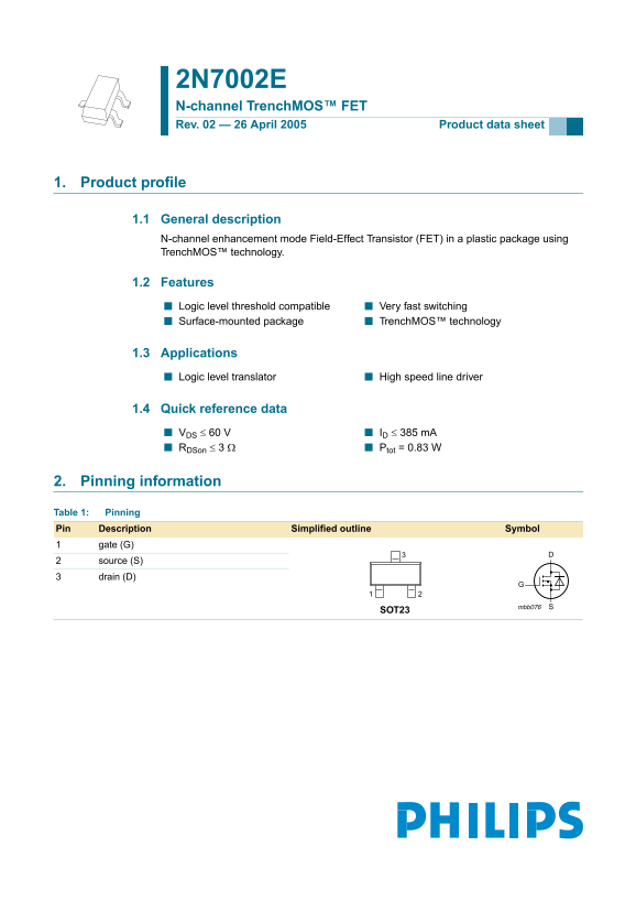
1.1 General description N-channel enhancement mode Field-Effect Transistor (FET) in a plastic package using Trench MOS™ technology.

1.2 Features Logic level threshold compatible Very fast switching Surface-mounted package Trench MOS™ technology

1.3 Applications Logic level translator High speed line driver

1.4 Quick reference data VDS ID m A

RDSon Ptot 0.83

2. Pinning information Table 1: Pinning Pin Description Simplified outline Symbol

gate (G) source (S) drain (D)

mbb076

SOT23

Page Summary Contents For Philips 2N7002E Data Sheet

Page 1 2N7002E N-channel Trench MOS™ FET Rev. 02 — 26 April 2005 Product data sheet 1. Product profile 1.1 General description N-channel enhancement mode Field-Effect Transistor (FET) in a plastic package us...
Page 2 Philips Semiconductors 2N7002E N-channel Trench MOS™ FET 3. Ordering information Table 2: Ordering information Type number Package Name Description Version 2N7002E TO-236AB plastic surface mounted pac...
Page 3 Philips Semiconductors 2N7002E N-channel Trench MOS™ FET 03aa17 03aa25 Tsp (°C) Tsp (°C) Ptot ID Pder %×= Ider %×= tot C°( C°( Fig 1. Normalized total power dissipation as a Fig 2. Normalized continuo...
Page 4 Philips Semiconductors 2N7002E N-channel Trench MOS™ FET 5. Thermal characteristics Table 4: Thermal characteristics Symbol Parameter Conditions Min Typ Max Unit Rth(j-sp) thermal resistance from junc...
Page 5 Philips Semiconductors 2N7002E N-channel Trench MOS™ FET 6. Characteristics Table 5: Characteristics Tj °C unless otherwise specified. Symbol Parameter Conditions Min Typ Max Unit Static characteristi...
Page 6 Philips Semiconductors 2N7002E N-channel Trench MOS™ FET 03ai12 03ai14 Tj = 25 °C VGS (V) = VGS (V) = 3.5 Tj = 25 °C ID (A) RDSon VDS (V) ID (A) Tj °C Tj °C Fig 5. Output characteristics: drain curren...
Page 7 Philips Semiconductors 2N7002E N-channel Trench MOS™ FET 03aa34 03aa37 VGS(th) ID (V) (A) typmin Tj (°C) VGS (V) ID m A; VDS VGS Tj °C; VDS Fig 9. Gate-source threshold voltage as a function of Fig 10...
Page 8 Philips Semiconductors 2N7002E N-channel Trench MOS™ FET 7. Package outline Plastic surface mounted package; 3 leads SOT23 e1 bp Lp detail X scale DIMENSIONS (mm are the original dimensions) UNIT bp E...
Page 9 Philips Semiconductors 2N7002E N-channel Trench MOS™ FET 8. Revision history Table 6: Revision history Document ID Release date Data sheet status Change notice Doc. number Supersedes 2N7002E_2 Product...
Page 10 Philips Semiconductors 2N7002E N-channel Trench MOS™ FET 9. Data sheet status Level Data sheet status Product status Definition Objective data Development This data sheet contains data from the object...
Page 11 Philips Semiconductors 2N7002E N-channel Trench MOS™ FET 14. Contents Product profile . . . . . . . . . . . . . . . . . . . . . . . . . . 1.1 General description. . . . . . . . . . . . . . . . . . . ....

Manual Details

Brand Philips
Pages 11
File Size 81.37 KB
Published June 20, 2026
1 views

Enter the captcha to get the download link:

captcha

Frequently Asked Questions

What package does the 2N7002E use?

TO-236AB plastic surface mounted package with 3 leads (SOT23).

What are common applications for this FET?

Logic level translator and high speed line driver.

What is the maximum continuous drain current?

385 mA at 25 °C when V_GS=10V.

What is the thermal resistance from junction to solder point?

Maximum is 150 K/W.