# A B C D E F G H I J K L M N O P Q R S T U V W X Y Z

Cypress CY7B923CY7B933 HotLink™ Transmitter Receiver Datasheet Manual

Summary

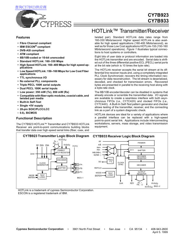
The CY7B923/CY7B933 HOTLink transceivers are high-speed, point-to-point serial data link components designed for robust interconnection of servers, workstations, and storage systems. These modules facilitate flexible connectivity across multiple standards (up to 400 Mbps), effectively replacing traditional parallel interfaces with reliable digital transmission solutions. This manual provides comprehensive technical documentation, including pinouts, detailed specifications, and connection diagrams, making it an essential resource for engineers integrating high-performance data networking equipment.
📄 Preview PAGE OF 35

Page 1 Text Content

查询CY7B923供应商

CY7B923 CY7B933

HOTLink™ Transmitter/Receiver Features twisted pair). Standard HOTLink data rates range from 160-330 Mbits/second. Higher speed HOTLink is also avail-

Fibre Channel compliant able for high speed applications (160-400 Mbits/second), as

IBM ESCON® compliant well as for those Low Cost applications HOTLink-155 (150-160 Mbits/second operations). Figure 1 illustrates typical connec-

DVB-ASI compliant

tions to host systems or controllers.

ATM compliant

Eight bits of user data or protocol information are loaded into

8B/10B-coded or 10-bit unencoded

the HOTLink transmitter and are encoded. Serial data is shift-

Standard HOTLink: 160–330 Mbps

ed out of the three differential positive ECL (PECL) serial ports

High Speed HOTLink: 160–400 Mbps for high speed ap-

at the bit rate (which is 10 times the byte rate).

plications

The HOTLink receiver accepts the serial bit stream at its dif-

Low Speed HOTLink: 150–160 Mbps for Low Cost Fiber

ferential line receiver inputs and, using a completely integrated

applications

PLL Clock Synchronizer, recovers the timing information nec-

TTL synchronous I/O

essary for data reconstruction. The bit stream is deserialized,

No external PLL components

decoded, and checked for transmission errors. Recovered

Triple PECL 100K serial outputs bytes are presented in parallel to the receiving host along with

Dual PECL 100K serial inputs a byte-rate clock.

Low power: 350 m W (Tx), 650 m W (Rx) The 8B/10B encoder/decoder can be disabled in systems that

Compatible with fiber-optic modules, coaxial cable, and already encode or scramble the transmitted data. I/O signals twisted pair media are available to create a seamless interface with both asyn- chronous FIFOs (i.e., CY7C42X) and clocked FIFOs (i.e.,

Built-In Self-Test

CY7C44X). A Built-In Self-Test pattern generator and checker

Single +5V supply

allows testing of the transmitter, receiver, and the connecting

28-pin SOIC/PLCC/LCC

link as a part of a system diagnostic check.

0.8µ Bi CMOS

HOTLink devices are ideal for a variety of applications where a parallel interface can be replaced with a high-speed

Functional Description

point-to-point serial link. Applications include interconnecting The CY7B923 HOTLink™ Transmitter and CY7B933 HOTLink workstations, servers, mass storage, and video transmission Receiver are point-to-point communications building blocks equipment.

that transfer data over high-speed serial links (fiber, coax, and

CY7B923 Transmitter Logic Block Diagram CY7B933 Receiver Logic Block Diagram

SC/D (Da) D0− RF

(Db h) FRAMER

SVS(Dj) A/B

ENAENNRP

ENABLE DATAINA−

SHIFTER

INPUT REGISTER INB(INB+)

SI(INB−

DECODER REGISTER

ENCODER PECL SO TTL

CLOCK CLOCK GENERATOR OUTA SYNC DECODER

SHIFTER OUTB REFCLK

OUTC OUTPUT

MODE TEST

REGISTER

MODE TEST LOGIC

BISTEN

BISTEN LOGIC

CKR RDY RVS(Qj)

(Qb h)

SC/D(Qa) B923–2

HOTLink is a trademark of cypress Semiconductor Corporation. ESCON is a registered trademark of IBM.

Cypress Semiconductor Corporation North First Street San Jose CA 95134 408-943-2600

April 5, 1999

Page Summary Contents For Cypress CY7B923CY7B933 HotLink™ Transmitter Receiver Datasheet Manual

Page 1 查询CY7B923供应商 CY7B923 CY7B933 HOTLink™ Transmitter/Receiver Features twisted pair). Standard HOTLink data rates range from 160-330 Mbits/second. Higher speed HOTLink is also avail- Fibre Channel compli...
Page 2 CY7B923 CY7B933 LO IC (D ITT SERIAL LINK HOSTB923–3 Figure 1. HOTLink System Connections CY7B923 Transmitter Pin Configurations CY7B933 Receiver Pin Configurations Top View Top View OUTB− OUTB+ INA− I...
Page 3 CY7B923 CY7B933 Maximum Ratings (Above which the useful life may be impaired. For user guide- Static Discharge Voltage >4001V lines, not tested.) (per MIL−STD−883, Method 3015) Storage Temperature ...
Page 4 CY7B923 CY7B933 CY7B923 HOTLink Transmitter (continued) Name I/O Description OUTA± PECL Out Differential Serial Data Outputs. These PECL 100K outputs (+5V referenced) are capable of driving OUTB± term...
Page 5 CY7B923 CY7B933 CY7B933 HOTLink Receiver (continued) Name I/O Description INB PECL in Serial Data Input B. This pin is either a single-ended PECL data receiver (INB) or half of the INB (INB+) (Diff In...
Page 6 CY7B923 CY7B933 table. If SC/D is LOW, the data inputs are converted using the Data pulse stream will insure correct data transfers between asynchro- code table. If a byte time passes with the inputs ...
Page 7 CY7B923 CY7B933 The REFCLK input provides a byte-rate reference frequency Decoder to improve PLL acquisition time and limit unlocked frequency Parallel data is transformed from ANSI-specified X3.230 e...
Page 8 CY7B923 CY7B933 CY7B923/CY7B933 Electrical Characteristics Over the Operating Range[1] Parameter Description Test Conditions Min. Max. Unit TTL OUTs, CY7B923: RP; CY7B933: Q0−7, SC/D, RVS, RDY, CKR, S...
Page 9 CY7B923 CY7B933 Capacitance[7] Parameter Description Test Conditions Max. Unit CIN Input Capacitance TA = 25°C, f0 = 1 MHz, VCC = 5.0V p F AC Test Loads and Waveforms OUTPUT R1 R1=910 RL =50 R2=510 CL...
Page 10 CY7B923 CY7B933 Receiver Switching Characteristics Over the Operating Range[1] Parameter Description Max Min. Max. Min. Max. Unit Min. t CKR Read Clock Period (No Serial Data Input), REFCLK −1 +1 −1 +...
Page 11 CY7B923 CY7B933 Switching Waveforms for the CY7B923 HOTLink Transmitter t CKW t CPWH t CPWL t SENP t SD t HENP NOTES 10,11 D0–D7, SC/D, VALID DATA SVS, BISTEN t SD t HD DISABLED t PDF ENABLED t PDR t ...
Page 12 CY7B923 CY7B933 Switching Waveforms for the CY7B933 HOTLink Receiver t CKR t CPRH t CPRL t PRH t RH t PRF t A t ROH t H SC/D,RVS, t CKX t CPXL t CPXH REFCLK SI VBB SO 1.5VNOTE Static Alignment Error-F...
Page 13 CY7B923 CY7B933 DATA LATCHED IN TRANSMITTER LATENCY t B 10ns D0−7, SC/D, DATA SVS K28.5 K28.5 DATAOUTX± DATA SENT Figure 2. CY7B923 Transmitter Data Pipeline ceiver on the INx± inputs. The receiver PL...
Page 14 CY7B923 CY7B933 CKR STRETCHES AS RF LATCHED ON DATA BOUNDARY CHANGES FALLING EDGE OF CKR Q0−7, SC/D, DATADATADATADATADATA K28.5 DATA DATA RVS RDY RDY IS HIGH WHILE WAITING FOR K28.5 RDY IS LOW RDY RES...
Page 15 CY7B923 CY7B933 CLOCKED FIFOASYNCHRONOUS FIFO Q0 ENR Q0 8CKR ENA RP D0 7,SC/DCKW ENN D0 7,SC/DCKWF HOTLINK TRANSMITTER HOTLINK TRANSMITTER HOTLINK RECEIVER HOTLINK RECEIVER Q0 7,SC/DCKR RDY Q0 7,SC/DC...
Page 16 CY7B923 CY7B933 In systems that require the outputs to be shut off during some rial data output is controlled by an internal Phase-Locked Loop periods when link transmission is prohibited (e.g., for l...
Page 17 CY7B923 CY7B933 CY7B923 DON'T CARE DON'T CARE BIST WITHIN SPEC. LOOP CKW DON'T CARE DON'T CARE Tx Tx START STOP BISTEN CY7B933 WITHIN SPEC. REFCLK DON'T CARE DON'T CARE SC/D INA ERROR TEST BIST START ...
Page 18 CY7B923 CY7B933 mitter BIST loop to run while the Receiver runs in normal CY7B933 HOTLink Receiver Operating Mode mode. The BIST loop includes deliberate violation symbols Description and will adequat...
Page 19 CY7B923 CY7B933 er PLL data synchronizer (one per 10 bit byte) and that it be com- RVS SC/D Qouts Name patible with the transmission media. 1. Good Data code received The framer function in Bypass mod...
Page 20 CY7B923 CY7B933 Receiver Test Mode Description logic and test pattern inputs can be synchronized by sending a SYNC pattern and allowing the Framer to align the logic to The CY7B933 Receiver offers two...
Page 21 CY7B923 CY7B933 To clarify this correspondence, the following example shows Transmission Order the conversion from an FC-2 Valid Data Byte to a Transmission Within the definition of the 8B/10B Transmi...
Page 22 CY7B923 CY7B933 negative at the end of the 6-bit sub-block if the 6-bit ceiver’s current running disparity for the next received Trans- sub-block is 111000, and it is negative at the end of the 4-bit ...
Page 23 CY7B923 CY7B933 Valid Data Characters (SC/D = LOW) Data Bits Current RD− Current RD+ Byte Name HGF EDCBA abcdei fghj abcdei fghj D0.0
Page 24 CY7B923 CY7B933 Valid Data Characters (SC/D = LOW) (continued) Data Bits Current RD− Current RD+ Byte Name HGF EDCBA abcdei fghj abcdei fghj D0.1
Page 25 CY7B923 CY7B933 Valid Data Characters (SC/D = LOW) (continued) Data Bits Current RD− Current RD+ Byte Name HGF EDCBA abcdei fghj abcdei fghj D2.2
Page 26 CY7B923 CY7B933 Valid Data Characters (SC/D = LOW) (continued) Data Bits Current RD− Current RD+ Byte Name HGF EDCBA abcdei fghj abcdei fghj D0.3
Page 27 CY7B923 CY7B933 Valid Data Characters (SC/D = LOW) (continued) Data Bits Current RD− Current RD+ Byte Name HGF EDCBA abcdei fghj abcdei fghj D0.4
Page 28 CY7B923 CY7B933 Valid Data Characters (SC/D = LOW) (continued) Data Bits Current RD− Current RD+ Byte Name HGF EDCBA abcdei fghj abcdei fghj D0.5
Page 29 CY7B923 CY7B933 Valid Data Characters (SC/D = LOW) (continued) Data Bits Current RD− Current RD+ Byte Name HGF EDCBA abcdei fghj abcdei fghj D3.6
Page 30 CY7B923 CY7B933 Valid Data Characters (SC/D = LOW) (continued) Data Bits Current RD− Current RD+ Byte Name HGF EDCBA abcdei fghj abcdei fghj D0.7
Page 31 CY7B923 CY7B933 Valid Special Character Codes and Sequences (SC/D = HIGH)[23, 24] Bits Current RD− Current RD+ S.C. Byte Name S.C. Code Name HGF EDCBA abcdei fghj abcdei fghj K28.0 C0.0 (C00) K28.1 C1...
Page 32 CY7B923 CY7B933 Ordering Information Package Operating Speed Ordering Code Name Package Type Range Standard CY7B923-JC J64 28-Lead Plastic Leaded Chip Carrier Commercial CY7B923-JI J64 28-Lead Plastic...
Page 33 CY7B923 CY7B933 MILITARY SPECIFICATIONS Group A Subgroup Testing Switching Characteristics Parameter Subgroup t CKW 9, 10, 11 DC Characteristics Parameter Subgroup t CPWH 9, 10, 11 VOHT 1, 2, 3 t CPWL...
Page 34 CY7B923 CY7B933 Package Diagrams 28-Lead Plastic Leaded Chip Carrier J64 28-Square Leadless Chip Carrier L64 MIL-STD-1835 C-4
Page 35 CY7B923 CY7B933 Package Diagrams (continued) 28-Lead (300-Mil) Molded SOIC S21 © Cypress Semiconductor Corporation, 1999. The information contained herein is subject to change without notice. Cypress ...

Manual Details

Brand Cypress
Pages 35
File Size 623.62 KB
Published May 18, 2026
104 views

Enter the captcha to get the download link:

captcha

Frequently Asked Questions

What speeds are available for HOTLink data rates?

Standard rates range from 160–330 Mbps; high speed can reach 160–400 Mbps, and low cost options run at 150–160 Mbps.

Does the receiver need external timing components?

No, the HOTLink receiver uses a completely integrated PLL Clock Synchronizer to recover necessary timing information.

What types of media can be used for connectivity?

Compatible media include fiber-optic modules, coaxial cable, and twisted pair.

Can the device generate its own clock signal for testing?

Yes, it includes a Built-In Self-Test pattern generator that allows the testing of all components using a single +5V supply.