# A B C D E F G H I J K L M N O P Q R S T U V W X Y Z

ATMEL AT45DB011B User Guide

Summary

This low-power Serial Peripheral Interface (SPI) Flash memory is engineered for reliable data and code storage in demanding commercial and industrial embedded systems. Featuring 1MB of non-volatile memory and an integrated SRAM buffer, it supports efficient programmability without requiring high voltages. The accompanying manual provides comprehensive details on the device's architecture, including sector, block, and page programming methods. It guides developers through utilizing the simple three-wire interface (CS/SCK/SI) for optimal integration, ensuring robust system reliability in low-voltage applications.
📄 Preview 📖 Table of Contents Contents PAGE OF 32

Page 1 Text Content

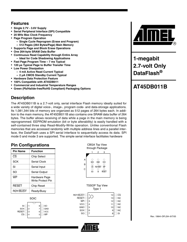
Features Single 2.7V - 3.6V Supply Serial Peripheral Interface (SPI) Compatible 20 MHz Max Clock Frequency Page Program Operation Single Cycle Reprogram (Erase and Program) 512 Pages (264 Bytes/Page) Main Memory Supports Page and Block Erase Operations One 264-byte SRAM Data Buffer Continuous Read Capability through Entire Array Ideal for Code Shadowing Applications 1-megabit Fast Page Program Time – 7 ms Typical 120 µs Typical Page to Buffer Transfer Time

2.7-volt Only

Low Power Dissipation 4 m A Active Read Current Typical

Data Flash®

2 µA CMOS Standby Current Typical Hardware Data Protection Feature 100% Compatible with AT45DB011 Commercial and Industrial Temperature Ranges

AT45DB011B

Green (Pb/Halide-free/Ro HS Compliant) Packaging Options

Description The AT45DB011B is a 2.7-volt only, serial interface Flash memory ideally suited for wide variety of digital voice-, image-, program code- and data-storage applications. Its 1,081,344 bits of memory are organized as 512 pages of 264 bytes each. In addi- tion to the main memory, the AT45DB011B also contains one SRAM data buffer of 264 bytes. The buffer allows receiving of data while a page in the main memory is being reprogrammed. EEPROM emulation (bit or byte alterability) is easily handled with a self-contained three step Read-Modify-Write operation. Unlike conventional Flash memories that are accessed randomly with multiple address lines and a parallel inter- face, the Data Flash uses a SPI serial interface to sequentially access its data. SPI mode 0 and mode 3 are supported. The simple serial interface facilitates hardware

Pin Configurations CBGA Top View through Package

Pin Name Function

AT45DB011B

CS Chip Select

SCK Serial Clock SCK GND VCC Preliminary 16-

SI Serial Input CS RDY/BSY WP

Megabit 2.7-volt

SO Serial Output SO SI RESET

Only Serial

WP Hardware Page

Write Protect Pin

Data Flash

RESET Chip Reset TSSOP Top View Type 1

RDY/BUSY Ready/Busy

RDY/BUSY CS SOIC RESET NC WP NC VCC NC

SI SO

GND NC

SCK GND

SCK NC

RESET VCC

SO SI

CS WP

Rev. 1984I–DFLSH–9/7/05

Page Summary Contents For ATMEL AT45DB011B User Guide

Page 1 Features Single 2.7V - 3.6V Supply Serial Peripheral Interface (SPI) Compatible 20 MHz Max Clock Frequency Page Program Operation Single Cycle Reprogram (Erase and Program) 512 Pages (264 Bytes/Page) ...
Page 2 layout, increases system reliability, minimizes switching noise, and reduces package size and active pin count. The device is optimized for use in many commercial and industrial applica- tions where h...
Page 3 AT45DB011B Memory Architecture Diagram SECTOR ARCHITECTURE BLOCK ARCHITECTURE PAGE ARCHITECTURE SECTOR 0 SECTOR 0 = 2112 BYTES (2K + 64) 8 Pages BLOCK 0 BLOCK 1 BLOCK 2 BLOCK 3 SECTOR 1 = 65,472 BYTES...
Page 4 CONTINUOUS ARRAY READ: By supplying an initial starting address for the main memory array, the Continuous Array Read command can be utilized to sequentially read a continuous stream of data from the d...
Page 5 AT45DB011B STATUS REGISTER READ: The status register can be used to determine the device’s ready/busy status, the result of a Main Memory Page to Buffer Compare operation, or the device density. To re...
Page 6 BUFFER TO MAIN MEMORY PAGE PROGRAM WITHOUT BUILT-IN ERASE: A previously erased page within main memory can be programmed with the contents of the buffer. An 8-bit opcode of 88H is followed by the six ...
Page 7 AT45DB011B MAIN MEMORY PAGE PROGRAM THROUGH BUFFER: This operation is a combination of the Buffer Write and Buffer to Main Memory Page Program with Built-in Erase operations. Data is first shifted int...
Page 8 Absolute Maximum Ratings* Temperature under Bias -55°C to +125°C *NOTICE: Stresses beyond those listed under “Absolute Maximum Ratings” may cause permanent dam- Storage Temperature -65°C to +150°C age...
Page 9 AT45DB011B Operation Mode The modes described can be separated into two groups – modes which make use of the Flash Summary memory array (Group A) and modes which do not make use of the Flash memory ar...
Page 10 RESET: A low state on the reset pin (RESET) will terminate the operation in progress and reset the internal state machine to an idle state. The device will remain in the reset condition as long as a l...
Page 11 AT45DB011B Table 1. Read Commands Command SCK Mode Opcode Inactive Clock Polarity Low or High 68H Continuous Array Read SPI Mode 0 or 3 E8H Inactive Clock Polarity Low or High 52H Main Memory Page Rea...
Page 12 Table 4. Detailed Bit-level Addressing Sequence Address Byte Address Byte Address Byte Additional Don’t Care Bytes Opcode Opcode Required es er ve es er ve 52H 4 Bytes es er ve es er ve 54H 1 Byte es ...
Page 13 AT45DB011B DC Characteristics Symbol Parameter Condition Min Typ Max Units ISB Standby Current CS, RESET, WP = VIH, all inputs at µA CMOS levels ICC1 Active Current, Read Operation f = 20 MHz; IOUT = ...
Page 14 Input Test Waveforms and Measurement Levels AC AC DRIVING MEASUREMENT LEVELS LEVEL0.45V t R, t F < 3 ns (10% to 90%) Output Test Load DEVICE UNDER TEST AC Waveforms Two different timing diagrams ar...
Page 15 AT45DB011B Reset Timing (Inactive Clock Polarity Low Shown) t REC t CSS t RST RESET HIGH IMPEDANCE HIGH IMPEDANCE Note: The CS signal should be in the high state before the RESET signal is deasserted....
Page 16 Write The following block diagram and waveforms illustrate the various write sequences available. Operations FLASH MEMORY ARRAY PAGE (264 BYTES) BUFFER TO MAIN MEMORY PAGE PROGRAM BUFFER (264 BYTES) M...
Page 17 AT45DB011B Read The following block diagram and waveforms illustrate the various read sequences available. Operations FLASH MEMORY ARRAY PAGE (264 BYTES) MAIN MEMORY PAGE TO BUFFER MAIN MEMORY BUFFER ...
Page 18 Detailed Bit-level Read Timing – Inactive Clock Polarity Low Continuous Array Read (Opcode: 68H) DATA OUT LSB MSB HIGH-IMPEDANCE SO D7 D6 D5 D2 D1 D0 D7 D6 D5 BIT 2111 BIT 0 OF OF PAGE n PAGE n+1 Main...
Page 19 AT45DB011B Detailed Bit-level Read Timing – Inactive Clock Polarity Low (Continued) Buffer Read (Opcode: 54H) CS COMMAND OPCODE DATA OUT HIGH-IMPEDANCE SO D7 D6 D5 MSB Status Register Read (Opcode: 57...
Page 20 Detailed Bit-level Read Timing – Inactive Clock Polarity High Continuous Array Read (Opcode: 68H) CS DATA OUT LSB MSB HIGH-IMPEDANCE SO D7 D6 D5 D2 D1 D0 D7 D6 D5 BIT 2111 BIT 0 OF OF PAGE n PAGE n+1 ...
Page 21 AT45DB011B Detailed Bit-level Read Timing – Inactive Clock Polarity High (Continued) Buffer Read (Opcode: 54H) CS COMMAND OPCODE DATA OUT HIGH-IMPEDANCE SO D7 D6 D5 D4 MSB Status Register Read (Opcode...
Page 22 Detailed Bit-level Read Timing – SPI Mode 0 Continuous Array Read (Opcode: E8H) CS DATA OUT LSB MSB HIGH-IMPEDANCE SO D7 D6 D5 D2 D1 D0 D7 D6 D5 BIT 2111 BIT 0 OF OF PAGE n PAGE n+1 Main Memory Page R...
Page 23 AT45DB011B Detailed Bit-level Read Timing – SPI Mode 0 (Continued) Buffer Read (Opcode: D4H) CS COMMAND OPCODE DATA OUT HIGH-IMPEDANCE SO D7 D6 D5 D4 Status Register Read (Opcode: D7H) CS COMMAND OPCO...
Page 24 Detailed Bit-level Read Timing – SPI Mode 3 Continuous Array Read (Opcode: E8H) CS DATA OUT LSB MSB HIGH-IMPEDANCE SO D7 D6 D5 D2 D1 D0 D7 D6 D5 BIT 2111 BIT 0 OF OF PAGE n PAGE n+1 Main Memory Page R...
Page 25 AT45DB011B Detailed Bit-level Read Timing – SPI Mode 3 (Continued) Buffer Read (Opcode: D4H) CS COMMAND OPCODE DATA OUT HIGH-IMPEDANCE SO D7 D6 D5 D4 MSB Status Register Read (Opcode: D7H) CS COMMAND ...
Page 26 Figure 1. Algorithm for Sequentially Programming or Reprogramming the Entire Array START provide address and data BUFFER WRITE (84H) MAIN MEMORY PAGE PROGRAM BUFFER to MAIN MEMORY PAGE PROGRAM (83H) N...
Page 27 AT45DB011B Figure 2. Algorithm for Randomly Modifying Data START provide address of page to modify MAIN MEMORY PAGE If planning to modify multiple to BUFFER TRANSFER bytes currently stored within (53H...
Page 28 Ordering Information ICC (m A) f SCK (MHz) Standby Ordering Code Package Operation Range Active AT45DB011B-CC 9C1 Commercial 0.01 AT45DB011B-SC 8S2 (0°C to 70°C) AT45DB011B-XC 14X AT45DB011B-CI 9C1 In...
Page 29 AT45DB011B Packaging Information 9C1 – CBGA Dimensions in Millimeters and (Inches). Controlling dimension: Millimeters. A1 ID SIDE VIEW TOP VIEW 0.25(0.010)MIN 1.20(0.047)MAX 1.50(0.059) REF 2.0 (0.07...
Page 30 8S2 – EIAJ SOIC Top View End View COMMON DIMENSIONS (Unit of Measure = mm) SYMBOL MIN NOM MAX NOTE Side View L 0.51 0.85 ∅ 0° 8° e 1.27 BSC 4 Notes: 1. This drawing is for general information only; re...
Page 31 AT45DB011B 14X – TSSOP Dimensions in Millimeters and (Inches). Controlling dimension: Millimeters. JEDEC Standard MO-153 AB-1. INDEX MARK 1.20 (0.047) MAX 0.65 (.0256) BSC 0.15 (0.006) SEATING 0.30 (0...
Page 32 Atmel Corporation Atmel Operations 2325 Orchard Parkway Memory RF/Automotive San Jose, CA 95131, USA 2325 Orchard Parkway Theresienstrasse 2 Tel: 1(408) 441-0311 San Jose, CA 95131, USA Postfach 3535 ...

Manual Details

Brand Atmel
Pages 32
File Size 449.42 KB
Published May 15, 2026
206 views

Enter the captcha to get the download link:

captcha

Frequently Asked Questions

What external components are required to access the data?

The device uses a three-wire serial interface consisting of Serial Input (SI), Serial Output (SO), and the Serial Clock (SCK), controlled by the Chip Select pin (CS).

Does this chip require separate erase cycles before programming data?

No, all programming cycles are self-timed, and no separate erase cycle is required before programming.

What is the low current draw capability for standby mode?

The typical CMOS Standby Current is very low at 2 µA.