ANALOG DEVICES AD9410 Data Sheet manual instructions
Summary
The AD9410 is a high-performance, 10-bit Analog-to-Digital Converter (ADC) clocked up to 210 MSPS, engineered for demanding applications like radar, communications, and advanced imaging systems. This manual offers comprehensive technical documentation for system architects, detailing functional block diagrams, pin configurations, and advanced features such as integrated track-and-hold circuits and data synchronization inputs. It provides the necessary engineering depth to reliably implement complex, high-speed signal processing and acquisition solutions across an industrial temperature range.
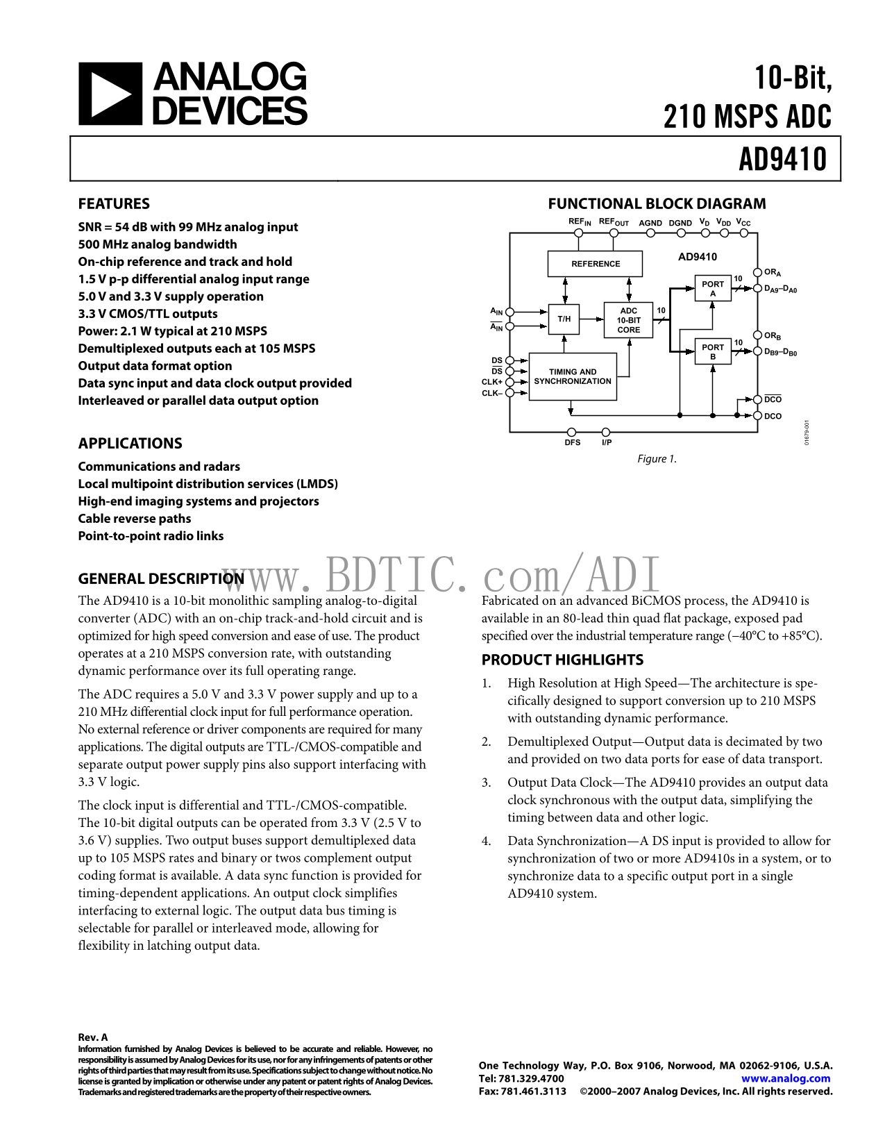
Page 1 Text Content
10-Bit, 210 MSPS ADC
AD9410 FEATURES FUNCTIONAL BLOCK DIAGRAM
REFIN REFOUT DGNDAGND VD VDD VCC
SNR = 54 d B with 99 MHz analog input 500 MHz analog bandwidth
AD9410
On-chip reference and track and hold REFERENCE
1.5 V p-p differential analog input range
DA9–DA0
5.0 V and 3.3 V supply operation
AIN 10ADC
3.3 V CMOS/TTL outputs
T/H 10-BIT
Power: 2.1 W typical at 210 MSPS CORE
Demultiplexed outputs each at 105 MSPS PORT
DB9–DB0
Output data format option
DS TIMING AND
CLK+ SYNCHRONIZATION
Data sync input and data clock output provided
Interleaved or parallel data output option DCO DCO
APPLICATIONS DFS I/P
Figure 1.
Communications and radars Local multipoint distribution services (LMDS) High-end imaging systems and projectors Cable reverse paths Point-to-point radio links
GENERAL DESCRIPTION www.BDTIC.com/ADI The AD9410 is a 10-bit monolithic sampling analog-to-digital Fabricated on an advanced Bi CMOS process, the AD9410 is converter (ADC) with an on-chip track-and-hold circuit and is available in an 80-lead thin quad flat package, exposed pad
optimized for high speed conversion and ease of use. The product specified over the industrial temperature range (−40°C to +85°C).
operates at a 210 MSPS conversion rate, with outstanding
PRODUCT HIGHLIGHTS
dynamic performance over its full operating range.
1. High Resolution at High Speed—The architecture is spe-
The ADC requires a 5.0 V and 3.3 V power supply and up to a
cifically designed to support conversion up to 210 MSPS
210 MHz differential clock input for full performance operation.
with outstanding dynamic performance.
No external reference or driver components are required for many
2. Demultiplexed Output—Output data is decimated by two
applications. The digital outputs are TTL-/CMOS-compatible and
and provided on two data ports for ease of data transport.
separate output power supply pins also support interfacing with 3.3 V logic. 3. Output Data Clock—The AD9410 provides an output data
clock synchronous with the output data, simplifying the
The clock input is differential and TTL-/CMOS-compatible. 9-
timing between data and other logic.
The 10-bit digital outputs can be operated from 3.3 V (2.5 V to 3.6 V) supplies. Two output buses support demultiplexed data 4. Data Synchronization—A DS input is provided to allow for up to 105 MSPS rates and binary or twos complement output synchronization of two or more AD9410s in a system, or to coding format is available. A data sync function is provided for synchronize data to a specific output port in a single timing-dependent applications. An output clock simplifies AD9410 system. interfacing to external logic. The output data bus timing is selectable for parallel or interleaved mode, allowing for flexibility in latching output data.
Rev. A Information furnished by Analog Devices is believed to be accurate and reliable. However, no responsibility is assumed by Analog Devices for its use, nor for any infringements of patents or other
One Technology Way, P.O. Box 9106, Norwood, MA 02062-9106, U.S.A.
rights of third parties that may result from its use. Specifications subject to change without notice. No
license is granted by implication or otherwise under any patent or patent rights of Analog Devices. Tel: 781.329.4700 www.analog.com Trademarks and registered trademarks are the property of their respective owners. Fax: 781.461.3113 ©2000–2007 Analog Devices, Inc. All rights reserved.
Page Summary Contents For ANALOG DEVICES AD9410 Data Sheet manual instructions
Manual Details
| Brand | Analog Devices |
|---|---|
| Pages | 20 |
| File Size | 439.25 KB |
| Published | July 16, 2026 |
Enter the captcha to get the download link:

Frequently Asked Questions
What is the maximum conversion rate of the AD9410 ADC?
The unit can operate at a conversion rate up to 210 MSPS.
What specific power supplies does the AD9410 require for operation?
It requires both a 5.0 V and 3.3 V power supply for proper operation.
How is data synchronization handled when using multiple units?
A Data Sync (DS) input is provided to allow for synchronization of two or more AD9410s in a system.
What flexibility is available for the digital output data bus?
The data output supports demultiplexed data on two ports, and the timing can be selectable for parallel or interleaved mode.