# A B C D E F G H I J K L M N O P Q R S T U V W X Y Z

ANALOG DEVICES AD7641 18-Bit, 2 MSPS SAR ADC User's Manual

Summary

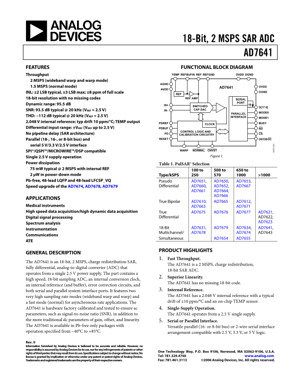
The AD7641 is a high-performance, 18-bit, 2 MSPS SAR Analog-to-Digital Converter designed for demanding signal acquisition. It offers superior linearity and operates efficiently from a single 2.5V power supply, featuring an internal reference and temperature sensor. This comprehensive manual provides detailed functional block diagrams, full technical specifications, and guidance on utilizing its versatile parallel and serial interfaces. Ideal for engineers developing advanced systems in medical instrumentation, high-speed data logging, spectrum analysis, and digital signal processing applications.
📄 Preview 📖 Table of Contents Contents PAGE OF 28

Page 1 Text Content

18-Bit, 2 MSPS SAR ADC

AD7641 FEATURES FUNCTIONAL BLOCK DIAGRAM

Throughput TEMP REFBUFIN REF REFGND DGNDDVDD

2 MSPS (wideband warp and warp mode)

1.5 MSPS (normal mode) AD7641 OVDD

INL: ±2 LSB typical, ±3 LSB max; ±8 ppm of full scale OGND

REF 18-bit resolution with no missing codes REF AMP

SERIAL PORT

Dynamic range: 95.5 d B IN+

SWITCHED

SNR: 93.5 d B typical @ 20 k Hz (VREF = 2.5 V) IN– CAP DAC

MODE0

PARALLEL

THD: −112 d B typical @ 20 k Hz (VREF = 2.5 V) INTERFACE

MODE1

2.048 V internal reference: typ drift 10 ppm/°C; TEMP output

PDREF CLOCK BUSY

Differential input range: ±VREF (VREF up to 2.5 V) PDBUF RD

CONTROL LOGIC AND

No pipeline delay (SAR architecture) PD CS

CALIBRATION CIRCUITRY

Parallel (18-, 16-, or 8-bit bus) and RESET D0/OB/2C

serial 5 V/3.3 V/2.5 V interface

SPI®/QSPI™/MICROWIRE™/DSP compatible WARP NORMAL CNVST

Single 2.5 V supply operation Figure 1.

Power dissipation

Table 1. Pul SAR® Selection

75 m W typical @ 2 MSPS with internal REF

100 to 500 to 650 to

2 μW in power-down mode Type/k SPS 1000 >1000 Pb-free, 48-lead LQFP and 48-lead LFCSP_VQ Pseudo AD7651, AD7650, AD7653,

Speed upgrade of the AD7674, AD7678, AD7679 Differential AD7660, AD7652, AD7667 AD7661 AD7664,

AD7666

APPLICATIONS

True Bipolar AD7610, AD7665 AD7612,

Medical instruments AD7663 AD7671 High speed data acquisition/high dynamic data acquisition True AD7675 AD7676 AD7677 AD7621,

Digital signal processing Differential AD7622,

AD7623

Spectrum analysis

18-Bit AD7631, AD7679 AD7634, AD7641,

Instrumentation

Multichannel/ AD7678 AD7674 AD7643

Communications

Simultaneous AD7654 AD7655

PRODUCT HIGHLIGHTS

GENERAL DESCRIPTION

1. Fast Throughput.

The AD7641 is an 18-bit, 2 MSPS, charge redistribution SAR,

The AD7641 is a 2 MSPS, charge redistribution,

fully differential, analog-to-digital converter (ADC) that

18-bit SAR ADC.

operates from a single 2.5 V power supply. The part contains a 1-

2. Superior Linearity.

high speed, 18-bit sampling ADC, an internal conversion clock,

The AD7641 has no missing 18-bit code.

an internal reference (and buffer), error correction circuits, and

both serial and parallel system interface ports. It features two 3. Internal Reference. very high sampling rate modes (wideband warp and warp) and The AD7641 has a 2.048 V internal reference with a typical

a fast mode (normal) for asynchronous rate applications. The -chip TEMP sensor. drift of ±10 ppm/°C and an on

AD7641 is hardware factory calibrated and tested to ensure ac Single-Supply Operation. 4. parameters, such as signal-to-noise ratio (SNR), in addition to The AD7641 operates from a 2.5 V single supply. the more traditional dc parameters of gain, offset, and linearity. 5.

Serial or Parallel Interface.

The AD7641 is available in Pb-free only packages with

Versatile parallel (16- or 8-bit bus) or 2-wire serial interf ace

operation specified from −40°C to +85°C.

arrangement compatible with 2.5 V, 3.3 V, or 5 V logic.

Rev. 0 Information furnished by Analog Devices is believed to be accurate and reliable. However, no responsibility is assumed by Analog Devices for its use, nor for any infringements of patents or other

One Technology Way, P.O. Box 9106, Norwood, MA 02062-9106, U.S.A.

rights of third parties that may result from its use. Specifications subject to change without notice. No

license is granted by implication or otherwise under any patent or patent rights of Analog Devices. Tel: 781.329.4700 www.analog.com Trademarks and registered trademarks are the property of their respective owners. Fax: 781.461.3113 ©2006 Analog Devices, Inc. All rights reserved.

Page Summary Contents For ANALOG DEVICES AD7641 18-Bit, 2 MSPS SAR ADC User's Manual

Page 1 18-Bit, 2 MSPS SAR ADC AD7641 FEATURES FUNCTIONAL BLOCK DIAGRAM Throughput TEMP REFBUFIN REF REFGND DGNDDVDD 2 MSPS (wideband warp and warp mode) 1.5 MSPS (normal mode) AD7641 OVDD INL: ±2 LSB typical...
Page 2 AD7641 TABLE OF CONTENTS Features Analog Inputs Applications....................................................................................... Multiplexed Inputs General Description Driver Amplif...
Page 3 AD7641 SPECIFICATIONS AVDD = DVDD = 2.5 V; OVDD = 2.3 V to 3.6 V; VREF = 2.5 V; all specifications TMIN to TMAX, unless otherwise noted. Table 2. Parameter Conditions Min Typ Max Unit RESOLUTION 18 Bi...
Page 4 AD7641 Parameter Conditions Min Typ Max Unit Turn-On Settling Time CREF = 10 μF 5 ms REFBUFIN Output Voltage REFBUFIN @ 25°C 1.19 V REFBUFIN Output Resistance 6.33 kΩ EXTERNAL REFERENCE PDREF = PDBUF ...
Page 5 AD7641 TIMING SPECIFICATIONS AVDD = DVDD = 2.5 V; OVDD = 2.3 V to 3.6 V; VREF = 2.5 V; all specifications TMIN to TMAX, unless otherwise noted. Table 3. Parameter Symbol Min Typ Max Unit CONVERSION AN...
Page 6 AD7641 Table 4. Serial Clock Timings in Master Read After Convert Mode DIVSCLK[1] 0 0 1 1 DIVSCLK[0] Symbol 0 1 0 1 Unit SYNC to SCLK First Edge Delay Minimum t18 0.5 3 3 3 ns Internal SCLK Period Min...
Page 7 AD7641 ABSOLUTE MAXIMUM RATINGS Table 5. Stresses above those listed under Absolute Maximum Ratings Parameter Rating may cause permanent damage to the device. This is a stress Analog Inputs/Outputs ra...
Page 8 AD7641 PIN CONFIGURATION AND FUNCTION DESCRIPTIONS AGND AGND PIN 1 AVDD IDENTIFIER CNVST MODE0 PD MODE1 RESET D0/OB/2C CS WARP AD7641 TOP VIEW NORMAL DGND (Not to Scale) D1/A0 BUSY D2/A1 D17 D3 D16 D4...
Page 9 AD7641 Pin No. Mnemonic Type1 Description 13 D6 DI/O When MODE[1:0] = 0, 1, or 2, this output is used as Bit 6 of the parallel port data output bus. or EXT/INT When MODE[1:0] = 3, (serial mode), seria...
Page 10 AD7641 Pin No. Mnemonic Type1 Description 25 to D[14:17] DO Bit 14 to Bit 17 of the parallel port data output bus. These pins are always outputs, regardless of the interface mode. 29 BUSY DO Busy Outp...
Page 11 AD7641 TERMINOLOGY Integral Nonlinearity Error (INL) Total Harmonic Distortion (THD) Linearity error refers to the deviation of each individual code THD is the ratio of the rms sum of the first five h...
Page 12 AD7641 (V EF TS IN (L SB TYPICAL PERFORMANCE CHARACTERISTICS 1F FE 3.0 1F FF 2.0 1F FF 1F FF 1.5 1F FF 1F FF 1.0 1F FF 0.5 0.5 1F FF 1F FF 1F FF 1F FF –0.5 1F FF –1.5 1F FF –1.0 –2.0 1F FF –1.5 1F FF ...
Page 13 AD7641 TH , H IC (d SN , S IN (d PL IT (d f F ul l S ca le f S = 2MSPS f S = 2MSPS f IN = 20.1k Hz f IN = 100.8k Hz SNR = 93.6d B SNR = 93d B THD = –116d B THD = –101d B –40 SFDR = 112d B –40 SFDR = 1...
Page 14 AD7641 VD , O VD (µ SN , S IN EF ER ED LL LE (d 95.0 DVDD OVDD = 2.5V, ALL MODES SINAD OVDD = 3.3V, ALL MODES PDREF = PDBUF = HIGH INPUT LEVEL (d B) SAMPLING RATE (SPS) Figure 17. SNR and SINAD vs. In...
Page 15 AD7641 APPPLICATIONS INFORMATION SWITCHES CONTROL LSBMSB SW+ CONTROL COMP LOGIC REFGND OUTPUT CODE LSBMSB CNVST Figure 21. ADC Simplified Schematic CIRCUIT INFORMATION comparator to become unbalanced....
Page 16 AD7641 (S tr ai gh t B in ar y) TRANSFER FUNCTIONS Using the OB/2C digital input, except in 18-bit interface mode, Table 8. Output Codes and Ideal Input Voltages the AD7641 offers two output codings: ...
Page 17 AD7641 TYPICAL CONNECTION DIAGRAM switches. CIN is typically 12 p F and is mainly the ADC sampling Figure 23 shows a typical connection diagram for the AD7641. capacitor. During the conversion phase, ...
Page 18 AD7641 Single-to-Differential Driver • The noise generated by the driver amplifier needs to be kept as low as possible to preserve the SNR and transition For applications using unipolar analog signals...
Page 19 AD7641 However, because the AD7641 has a fine lead pitch, guarding For applications that use multiple AD7641 devices, it is more this node is not practical. Therefore, in these industrial and effectiv...
Page 20 AD7641 PS (d POWER SUPPLY It should be noted that the digital interface remains active even during the acquisition phase. To reduce the operating digital The AD7641 uses three sets of power supply pin...
Page 21 AD7641 INTERFACES DIGITAL INTERFACE PARALLEL INTERFACE The AD7641 has a versatile digital interface that can be set up The AD7641 is configured to use the parallel interface for an as either a serial ...
Page 22 AD7641 CS = 0 SERIAL INTERFACE CNVST, t1 RD The AD7641 is configured to use the serial interface when MODE[1:0] = 3. The AD7641 outputs 18 bits of data, MSB first, on the SDOUT pin. This data is synch...
Page 23 AD7641 EXT/INT = 0 RDC/SDIN = 0 INVSCLK = INVSYNC = 0 DIVSCLK[1:0] = 0 CS, RD CNVST BUSY t28 SDOUT D17 D16 D2 D1 D0X Figure 35. Master Serial Data Timing for Reading (Read After Convert) EXT/INT = 0 R...
Page 24 AD7641 SLAVE SERIAL INTERFACE External Clock An example of the concatenation of two devices is shown in The AD7641 is configured to accept an externally supplied Figure 37. Simultaneous sampling is po...
Page 25 AD7641 EXT/INT = 1 INVSCLK = 0 RD = 0 SDOUT D17 D16 D1 D0D15 X17 X16X SDIN X17 X16 X15 X1 X0 Y17 Y16 Figure 38. Slave Serial Data Timing for Reading (Read After Convert) EXT/INT = 1 INVSCLK = 0 RD = 0...
Page 26 AD7641 SPI Interface (ADSP-219x) MICROPROCESSOR INTERFACING The AD7641 is ideally suited for traditional dc measurement Figure 40 shows an interface diagram between the AD7641 and applications support...
Page 27 AD7641 APPLICATION HINTS LAYOUT The DVDD supply of the AD7641 can be either a separate supply or come from the analog supply, AVDD, or from the While the AD7641 has very good immunity to noise on the ...
Page 28 AD7641 OUTLINE DIMENSIONS 0.60 MAX BSC SQ 0.45 PIN 1 TOP VIEW BSC SQ 0.20 (PINS DOWN) SEATING 0.05 0.08 MAX PLANE VIEW A 0.27 COPLANARITY 0.50 BSC 0.22 LEAD PITCH 0.17 VIEW A ROTATED 90° CCW COMPLIANT...

Manual Details

Brand Analog Devices
Pages 28
File Size 666.79 KB
Published June 16, 2026
6 views

Enter the captcha to get the download link:

captcha

Frequently Asked Questions

What is the maximum throughput rate of the AD7641?

It provides a fast throughput up to 2 MSPS.

What power supplies can this ADC operate with?

The AD7641 operates using a single 2.5 V power supply.

Does it support various interface standards?

Yes, it is compatible with versatile parallel (16- or 8-bit bus) or 2-wire serial interfaces for 2.5V, 3.3V, or 5V logic.

What is the guaranteed operating temperature range?

The device is specified for an operational temperature range of -40°C to +85°C.