# A B C D E F G H I J K L M N O P Q R S T U V W X Y Z

ANALOG DEVICES AD5722R AD5732R AD5752R Data Sheet Manual

Summary

These high-precision dual Digital-to-Analog Converters (DACs) deliver robust 12-, 14-, or 16-bit resolution via a serial interface, suitable for both unipolar and bipolar voltage outputs. Engineered for demanding industrial, automation, and process control applications, they ensure stability across a wide temperature range with integrated features like programmable output ranges and reference buffers. The manual provides expert guidance on configuration, advanced electrical characteristics, optimal system integration, and real-world application techniques for analog system designers and hardware engineers requiring high reliability ICs interfacing with microcontrollers and DSPs.
📄 Preview PAGE OF 32

Page 1 Text Content

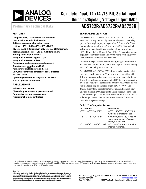
Complete, Dual, 12-/14-/16-Bit, Serial Input, Unipolar/Bipolar, Voltage Output DACs

Preliminary Technical Data AD5722R/AD5732R/AD5752R FEATURES GENERAL DESCRIPTION Complete, dual, 12-/14-/16-bit D/A converter The AD5722R/AD5732R/AD5752R are dual, 12-/14-/16-bit, Operates from single/dual supplies serial input, voltage output, digital-to-analog converters. They Software programmable output range operate from single supply voltages of +4.5 V up to +16.5 V or +5 V, +10 V, +10.8 V, ±5 V, ±10 V, ±10.8 V dual supply voltages from ±4.5 V up to ±16.5 V. Nominal full- INL error: ±16 LSB maximum, DNL error: ±1 LSB maximum scale output range is software-selectable from the options of Total unadjusted error (TUE): 0.1% FSR maximum +5 V, +10 V, +10.8 V, ±5 V, ±10 V, or ±10.8 V. Integrated output Settling time: 10 µs maximum amplifiers, reference buffers, and proprietary power-up/power- Integrated reference: 5 ppm/°C typ. down control circuitry are also provided. Integrated reference buffers

The parts offer guaranteed monotonicity, integral nonlinearity

Output control during power-up/brownout

(INL) of ±16 LSB maximum, low noise, 10 µs maximum settling

Simultaneous updating via LDAC

time, and an on-chip +2.5 V reference.

Asynchronous CLR to zero-/mid-scale

The AD5722R/AD5732R/AD5752R use a serial interface that

DSP-/microcontroller-compatible serial interface

operates at clock rates up to 30 MHz and are compatible with

24-lead TSSOP

Operating temperature range: −40°C to +85°C DSP and microcontroller interface standards. Double buffering i CMOS™ process technology1 allows the simultaneous updating of all DACs. The input coding is user-selectable twos complement or offset binary for a bipolar

APPLICATIONS

output (depending on the state of pin BIN/2s Comp), and

Industrial automation straight binary for a unipolar output. The asynchronous clear Closed-loop servo control, process control function clears all DAC registers to a user-selectable zero-scale Automotive test and measurement or mid-scale output. The parts are available in a 24-lead TSSOP Programmable logic controllers and offer guaranteed specifications over the −40°C to +85°C

industrial temperature range.

Table 1. Pin Compatible Devices Part Number Description AD5722/AD5732/AD5752 AD5722R/AD5732R/AD5752R

without internal reference.

AD5724/AD5734/AD5754 Complete, quad, 12-/14-/16-bit,

serial input, unipolar/bipolar, voltage output DAC.

AD5724R/AD5734R/AD5754R AD5724/AD5734/AD5754 with

internal reference.

1 For analog systems designers within industrial/instrumentation equipment OEMs who need high performance ICs at higher-voltage levels, i CMOS is a technology

platform that enables the development of analog ICs capable of 30 V and operating at ±15 V supplies while allowing dramatic reductions in power consumption and package size, and increased AC and DC performance.

Rev. Pr C Information furnished by Analog Devices is believed to be accurate and reliable. However, no responsibility is assumed by Analog Devices for its use, nor for any infringements of patents or other

One Technology Way, P.O. Box 9106, Norwood, MA 02062-9106, U.S.A.

rights of third parties that may result from its use. Specifications subject to change without notice. No

license is granted by implication or otherwise under any patent or patent rights of Analog Devices. Tel: 781.329.4700 www.analog.com Trademarks and registered trademarks are the property of their respective owners. Fax: 781.461.3113 ©2007 Analog Devices, Inc. All rights reserved.

Page Summary Contents For ANALOG DEVICES AD5722R AD5732R AD5752R Data Sheet Manual

Page 1 Complete, Dual, 12-/14-/16-Bit, Serial Input, Unipolar/Bipolar, Voltage Output DACs Preliminary Technical Data AD5722R/AD5732R/AD5752R FEATURES GENERAL DESCRIPTION Complete, dual, 12-/14-/16-bit D/A c...
Page 2 AD5722R/AD5732R/AD5752R Preliminary Technical Data TABLE OF CONTENTS Features Configuring the AD5722R/AD5732R/AD5752R.................. Applications.......................................................
Page 3 Preliminary Technical Data AD5722R/AD5732R/AD5752R FUNCTIONAL BLOCK DIAGRAM AVDDAVSS REFIN/REFOUT AD5722R/AD5732R/AD5752R DVCC 2.5V REFERENCE CLR REFERENCE BUFFERS BIN/2s COMP INPUT DAC SDIN DAC VOUTA...
Page 4 AD5722R/AD5732R/AD5752R Preliminary Technical Data SPECIFICATIONS DUAL SUPPLY SPECIFICATIONS AVDD = 4.5 V1 to 16.5 V, AVSS = −4.5 V1 to −16.5 V, GND = 0 V, REFIN= 2.5 V external, DVCC = 2.7 V to 5.5 V...
Page 5 Preliminary Technical Data AD5722R/AD5732R/AD5752R Parameter Value Unit Test Conditions/Comments OUTPUT CHARACTERISTICS2 Output Voltage Range ±10.8 V min to V max AVDD/AVSS = ±11.7 V min , REFIN = +2....
Page 6 AD5722R/AD5732R/AD5752R Preliminary Technical Data SINGLE SUPPLY SPECIFICATIONS AVDD = 4.5 V1 to 16.5 V, AVSS = 0 V, GND = 0 V, REFIN= 2.5 V external, DVCC = 2.7 V to 5.5 V RLOAD = 2 kΩ, CLOAD = 200 p...
Page 7 Preliminary Technical Data AD5722R/AD5732R/AD5752R Parameter Value Unit Test Conditions/Comments VOL, Output Low Voltage 0.4 V max DVCC = 2.7 V to 3.6 V, sinking 200 µA VOH, Output High Voltage DVCC −...
Page 8 AD5722R/AD5732R/AD5752R Preliminary Technical Data TIMING CHARACTERISTICS AVDD = 4.5 V to 16.5 V, AVSS = −4.5 V to −16.5 V / 0V, GND = 0 V, REFIN = 2.5 V external, DVCC = 2.7 V to 5.5 V RLOAD = 2 kΩ, ...
Page 9 Preliminary Technical Data AD5722R/AD5732R/AD5752R SDIN DB23 DB0 VOUTX VOUTX VOUTX Figure 2. Serial Interface Timing Diagram SDIN DB23 DB0 DB23 DB0 INPUT WORD FOR DAC N – 1INPUT WORD FOR DAC N t18 SDO...
Page 10 AD5722R/AD5732R/AD5752R Preliminary Technical Data SDIN DB23 DB0 DB23 DB0 NOP CONDITIONINPUT WORD SPECIFIES REGISTER TO BE READ SDO DB23 DB0 DB23 DB0 UNDEFINED SELECTED REGISTER DATA CLOCKED OUT Figur...
Page 11 Preliminary Technical Data AD5722R/AD5732R/AD5752R ABSOLUTE MAXIMUM RATINGS TA = 25°C unless otherwise noted. Transient currents of up to 100 m A do not cause SCR latch-up. Table 6. Stresses above tho...
Page 12 AD5722R/AD5732R/AD5752R Preliminary Technical Data PIN CONFIGURATION AND FUNCTION DESCRIPTIONS AVSS AVDD NC VOUTB VOUTA AD5722R/ NC AD5732R/ NC SIG_GND AD5752R BIN/2s COMP SIG_GND TOP VIEW NC (Not to ...
Page 13 Preliminary Technical Data AD5722R/AD5732R/AD5752R TYPICAL PERFORMANCE CHARACTERISTICS Figure 6. AD5752R Integral Nonlinearity Error vs. Code (Four Traces) Figure 9. AD5752R Differential Nonlinearity ...
Page 14 AD5722R/AD5732R/AD5752R Preliminary Technical Data Figure 12. AD5752R Integral Nonlinearity Error vs. Temperature (Four Traces) Figure 15. AD5752R Differential Nonlinearity Error vs. Supply Voltage (F...
Page 15 Preliminary Technical Data AD5722R/AD5732R/AD5752R Figure 18. AD5752R Total Unadjusted Error vs. Reference Voltage (Four Traces) Figure 21. AIDD vs. AVDD Figure 19. AD5752R Total Unadjusted Error vs. ...
Page 16 AD5722R/AD5732R/AD5752R Preliminary Technical Data Figure 24. Gain Error vs. Temperature (Four Traces) Figure 27. Full-Scale Settling Time, ±10 V Range (Two Traces) Figure 25. DICC vs. Logic Input Vol...
Page 17 Preliminary Technical Data AD5722R/AD5732R/AD5752R Figure 30. Full-Scale Settling Time, +5 V Range (Two Traces) Figure 33. Peak-to-Peak Noise, 100 k Hz Bandwidth (Four Traces) Figure 31. Digital-to-An...
Page 18 AD5722R/AD5732R/AD5752R Preliminary Technical Data Figure 36. REFOUT Output Noise (100 k Hz Bandwidth) Figure 39. REFOUT Load Transient (Two Traces) Figure 37. REFOUT Output Noise (0.1 Hz to 10 Hz Ban...
Page 19 Preliminary Technical Data AD5722R/AD5732R/AD5752R TERMINOLOGY Slew Rate Relative Accuracy or Integral Nonlinearity (INL) The slew rate of a device is a limitation in the rate of change of For the DAC...
Page 20 AD5722R/AD5732R/AD5752R Preliminary Technical Data DC Crosstalk DAC-to-DAC Crosstalk This is the dc change in the output level of one DAC in response DAC-to-DAC Crosstalk is the glitch impulse transfe...
Page 21 Preliminary Technical Data AD5722R/AD5732R/AD5752R THEORY OF OPERATION REFIN The AD5722R/AD5732R/AD5752R are dual, 12-/14-/16-bit, serial input, unipolar/bipolar, voltage output DACs. They operate fro...
Page 22 AD5722R/AD5732R/AD5752R Preliminary Technical Data Standalone Operation write cycle. SCLK is continuously applied to the input shift register when SYNC is low. If more than 24 clock pulses are The ser...
Page 23 Preliminary Technical Data AD5722R/AD5732R/AD5752R LOAD DAC (LDAC) CONFIGURING THE AD5722R/AD5732R/AD5752R After data has been transferred into the input register of the When the power supplies are ap...
Page 24 AD5722R/AD5732R/AD5752R Preliminary Technical Data Ideal Output Voltage to Input Code Relationship—AD5752R Table 9. Bipolar Output, Offset Binary Coding Digital Input Analog Output MSB LSB ±5 V Output...
Page 25 Preliminary Technical Data AD5722R/AD5732R/AD5752R Ideal Output Voltage to Input Code Relationship—AD5732R Table 12. Bipolar Output, Offset Binary Coding Digital Input Analog Output MSB LSB ±5 V Outpu...
Page 26 AD5722R/AD5732R/AD5752R Preliminary Technical Data Ideal Output Voltage to Input Code Relationship—AD5722R Table 15. Bipolar Output, Offset Binary Coding Digital Input Analog Output MSB LSB ±5 V Outpu...
Page 27 Preliminary Technical Data AD5722R/AD5732R/AD5752R INPUT REGISTER The input register is 24 bits wide and consists of a read/write bit, a reserved bit, three register select bits, three DAC address bit...
Page 28 AD5722R/AD5732R/AD5752R Preliminary Technical Data OUTPUT RANGE SELECT REGISTER The output range select register is addressed by setting the three REG bits to 001. The DAC address bits select the DAC ...
Page 29 Preliminary Technical Data AD5722R/AD5732R/AD5752R POWER CONTROL REGISTER The power control register is addressed by setting the three REG bits to 010. This register allows the user to control and det...
Page 30 AD5722R/AD5732R/AD5752R Preliminary Technical Data FEATURES Constant Current Clamp (CLAMP ENABLE = 1) ANALOG OUTPUT CONTROL If a short circuit occurs in this configuration, the current is In many indu...
Page 31 Preliminary Technical Data AD5722R/AD5732R/AD5752R APPLICATIONS INFORMATION GALVANICALLY ISOLATED INTERFACE +5V / ±5V OPERATION In many process control applications, it is necessary to provide When op...
Page 32 AD5722R/AD5732R/AD5752R Preliminary Technical Data OUTLINE DIMENSIONS EXPOSED 4.40 PAD 3.20 (Pins Up) 4.30 3.15 6.40 BSC TOP VIEW BOTTOM VIEW 1.20 MAX SEATING 0.09 PLANE 0.19 0.60 0.10 COPLANARITY 0.4...

Manual Details

Brand Analog Devices
Pages 32
File Size 295.82 KB
Published June 16, 2026
1 views

Enter the captcha to get the download link:

captcha

Frequently Asked Questions

What operating temperatures can the device withstand?

The parts are designed to operate within a temperature range of −40°C to +85°C.

Can this DAC support both single and dual voltage supplies?

Yes, it operates from single supply voltages up to +16.5V or dual supply voltages up to ±16.5V.

Is the output range selectable via software?

Yes, the scale output range is software-selectable from diverse options, including +5V, +10V, and ±10.8V.