# A B C D E F G H I J K L M N O P Q R S T U V W X Y Z

ADP1821 Analog Devices Data Sheet Manual

Summary

The ADP1821 is a high-performance, synchronous DC-to-DC step-down controller ideal for point-of-load power applications requiring extreme reliability. Featuring wide input voltage support (1V–24V) and built-in protections like soft start and thermal shutdown, it delivers efficient power regulation for complex systems. This resource provides detailed specifications and application guidance for engineers designing professional electronics in sectors like telecommunications, data servers, medical imaging, and industrial control.
📄 Preview 📖 Table of Contents Contents PAGE OF 24

Page 1 Text Content

Step-Down DC-to-DC Controller

ADP1821 FEATURES GENERAL DESCRIPTION Wide power-input voltage range: 1 V to 24 V The ADP1821 is a versatile and inexpensive, synchronous, Chip supply voltage range: 3.7 V to 5.5 V pulse-width-modulated (PWM), voltage-mode, step-down Wide output voltage range: 0.6 V to 85% of input voltage controller. It drives an all N-channel power stage to regulate an 1% accuracy, 0.6 V reference voltage output voltage as low as 0.6 V. The ADP1821 can be configured All N-channel MOSFET design for low cost to provide output voltages from 0.6 V to 85% of the input Fixed-frequency operation 300 k Hz, 600 k Hz, or voltage and is sized to handle large MOSFETs for point-of-load synchronized operation up to 1.2 MHz regulators. No current sense resistor required

The ADP1821 is well suited for a wide range of high power

Power-good output

applications, such as DSP and processor core power in telecom-

Programmable soft start with reverse current protection

munications, medical imaging, high performance servers, and

Soft start, thermal overload, current-limit protection

industrial applications. It operates from a 3.7 V to 5.5 V supply

Undervoltage lockout

0- with a power input voltage ranging from 1.0 V to 24 V.

10 μA shutdown supply current

The ADP1821 operates at a pin-selectable, fixed switching

Small, 16-lead QSOP

frequency of either 300 k Hz or 600 k Hz, minimizing external

APPLICATIONS

component size and cost. For noise sensitive applications, it

Telecommunications and networking systems EF FI IE can be synchronized to an external clock to achieve switching Set-top boxes frequencies between 300 k Hz and 1.2 MHz. The ADP1821 Printers includes soft start protection to limit the inrush current from Servers the input supply during startup, reverse current protection Medical imaging systems during soft start for precharged outputs, as well as a unique

Microprocessor and DSP core power supplies www.BDTIC.com/ADI adjustable lossless current-limit scheme utilizing external

Mobile communication base stations MOSFET sensing.

The ADP1821 operates over the –40°C to +125°C junction temperature range and is available in a 16-lead QSOP.

BIAS INPUT

5V TA = 25°C FREQUENCY = 300k Hz

10Ω D1 3.3V OUTPUT

POWER INPUT 2.5V TO 20V

VCC PVCC

1µF CIN1 CIN2 ADP1821 2.2µF 2.2µF 25V 25V

BST ×2

SHDN 0.47µF

DH M1

FREQ OUTPUT

SW 1.8V OUTPUT

SYNC 3.3kΩ

CSL COUT1 COUT2

PWGD M2 M3

DL 6.3V 2.5V 300Ω

PGND ×2 ×2

SS FB

GND 10n F

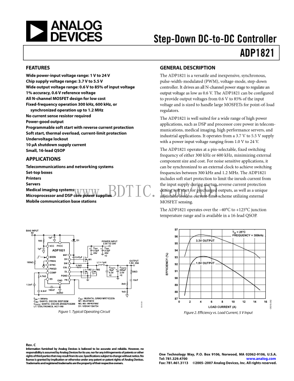
f SW = 300k Hz CIN1: MURATA, GRM31MR71E225k CIN2: SANYO, OSCON 20SP180M M1: IRLR7807Z COUT2: SANYO, OSCON 2R5SEPC820M M2, M3: IRFR3709Z L1: COILTRONICS, HC7-1R0 D1: VISHAY BAT54 LOAD CURRENT (A)

Figure 1. Typical Operating Circuit

Figure 2. Efficiency vs. Load Current, 5 V Input

Rev. C Information furnished by Analog Devices is believed to be accurate and reliable. However, no responsibility is assumed by Analog Devices for its use, nor for any infringements of patents or other

One Technology Way, P.O. Box 9106, Norwood, MA 02062-9106, U.S.A.

rights of third parties that may result from its use. Specifications subject to change without notice. No

license is granted by implication or otherwise under any patent or patent rights of Analog Devices. Tel: 781.329.4700 www.analog.com Trademarks and registered trademarks are the property of their respective owners. Fax: 781.461.3113 ©2005–2007 Analog Devices, Inc. All rights reserved.

Page Summary Contents For ADP1821 Analog Devices Data Sheet Manual

Page 1 Step-Down DC-to-DC Controller ADP1821 FEATURES GENERAL DESCRIPTION Wide power-input voltage range: 1 V to 24 V The ADP1821 is a versatile and inexpensive, synchronous, Chip supply voltage range: 3.7 V...
Page 2 ADP1821 TABLE OF CONTENTS Features Compensation............................................................................. Applications..................................................................
Page 3 ADP1821 SPECIFICATIONS VVCC = VPVCC = VSHDN = VFREQ = 5 V, SYNC = GND. All limits at temperature extremes are guaranteed via correlation using standard statistical quality control (SQC). TJ = −40°C to...
Page 4 ADP1821 Parameter Conditions Min Typ Max Unit LOGIC THRESHOLDS (SHDN, SYNC, FREQ) SHDN, SYNC, FREQ Input High Voltage VVCC = 3.7 V to 5.5 V 2.0 V SHDN, SYNC, FREQ Input Low Voltage VVCC = 3.7 V to 5.5...
Page 5 ADP1821 ABSOLUTE MAXIMUM RATINGS Stresses above those listed under Absolute Maximum Ratings Table 2. may cause permanent damage to the device. This is a stress Parameter Rating rating only; functional...
Page 6 ADP1821 PIN CONFIGURATION AND FUNCTION DESCRIPTIONS BST PVCC DH DL SW ADP1821 PGND TOP VIEW SYNC CSL (Not to Scale) FREQ VCC SHDN COMP PWGD FB GND SS Figure 4. Pin Configuration Table 3. Pin Function ...
Page 7 ADP1821 VC EN (µ EF FI IE EF FI IE TYPICAL PERFORMANCE CHARACTERISTICS TA = 25°C FREQUENCY = 300k Hz 3.3V OUTPUT 1.8V OUTPUT LOAD CURRENT (A) TEMPERATURE (°C) Figure 5. Efficiency vs. Load Current, VI...
Page 8 ADP1821 OUTPUT VOLTAGE (1V/DIV) OUTPUT VOLTAGE (50m V/DIV) SHDN (5V/DIV) INPUT VOLTAGE PWGD (5V/DIV) (5V/DIV) Figure 11. Line Transient Response, 10 V to 16 V Figure 13. Power-On Response, Prebiased O...
Page 9 ADP1821 THEORY OF OPERATION The ADP1821 is a versatile, economical, synchronous-rectified, control loop. A detailed design procedure for compensating the fixed-frequency, PWM, voltage mode step-down c...
Page 10 ADP1821 MOSFET DRIVERS SETTING THE OUTPUT VOLTAGE The DH pin drives the high-side switch MOSFET. This is a The output voltage is set using a resistive voltage divider from boosted 5 V gate driver that...
Page 11 ADP1821 COMPENSATION THERMAL SHUTDOWN The control loop is compensated by an external series RC The ADP1821 controller does not generate much heat under network from COMP to FB and sometimes requires a...
Page 12 ADP1821 APPLICATION INFORMATION Use the following equation to choose the inductor value: SELECTING THE INPUT CAPACITOR The input current to a buck converter is a pulsed waveform. It is zero when the h...
Page 13 ADP1821 In the case of output capacitors where the impedance of the The total power dissipation of the high-side MOSFET is the ESR and ESL are small at the switching frequency, for instance, sum of al...
Page 14 ADP1821 SETTING THE CURRENT LIMIT ADP1821 The current-limit comparator measures the voltage across the DH VOUT low-side MOSFET to determine the load current. The current limit is set through the curre...
Page 15 ADP1821 LC FILTER BODE PLOT For initial practical designs, a good choice for the crossover frequency is 1/10 of the switching frequency; first calculate GAIN f LC f ESR f CO f SW SW (19) FREQUENCY CO ...
Page 16 ADP1821 Two common compensation schemes are used, which are (29) sometimes referred to as Type II or Type III compensation, CCR depending on whether the compensation design includes two CC HFI or thre...
Page 17 ADP1821 Solving for CI in Equation 33 yields Next calculate CI (35) (43) f R f R LCZ ZZ Use the larger value of CI from Equation 34 or Equation 35. Because of the finite output current drive of the er...
Page 18 ADP1821 SETTING THE SOFT START PERIOD The soft start period, t SS, is achieved when VCSS = 0.6 V or The ADP1821 uses an adjustable soft start to limit the output SS SS )(k1001V8.0V6.0 voltage ramp-up ...
Page 19 ADP1821 PCB LAYOUT GUIDELINE In any switching converter, there are some circuit paths that • Avoid long traces or large copper areas at the FB and CSL carry high d I/dt, which can create spikes and no...
Page 20 ADP1821 PGNDAGND VIA TO 2 LAYER SOME TRACES ARE OMITTED FOR CLARITY Figure 20. Top Layer Layout Example of Circuit (See Figure 23) Figure 21. Bottom Layer Layout Example of Circuit (See Figure 23) REC...
Page 21 ADP1821 APPLICATION CIRCUITS The ADP1821 controller can be configured to regulate an output Rubycon ZLG low-ESR series, can also be paralleled up at the with a load of more than 20 A if the power comp...
Page 22 ADP1821 The ADP1821 can also be configured to run with an input voltage input voltage from 12 V to 5 V to power the ADP1821. These higher than 5.5 V. Figure 23 shows a typical application circuit exte...
Page 23 ADP1821 OUTLINE DIMENSIONS PIN 1 BSC SEATING 0.010 COPLANARITY PLANE 0.006 COMPLIANT TO JEDEC STANDARDS MO-137-AB Figure 24. 16-Lead Shrink Small Outline Package [QSOP] (RQ-16) Dimensions shown in inc...
Page 24 ADP1821 NOTES www.BDTIC.com/ADI ©2005–2007 Analog Devices, Inc. All rights reserved. Trademarks and registered trademarks are the property of their respective owners. D05310-0-4/07(C) Rev. C | Page 24...

Manual Details

Brand Analog Devices
Pages 24
File Size 484.90 KB
Published June 15, 2026
2 views

Enter the captcha to get the download link:

captcha

Frequently Asked Questions

What is the input voltage range for the ADP1821 controller?

The device operates from a wide power-input voltage range spanning 1 V to 24 V.

How can I adjust the switching frequency?

It offers pin-selectable fixed switching frequencies of either 300 kHz or 600 kHz, and can be synchronized up to 1.2 MHz for specific applications.

Does the ADP1821 require external components like current sense resistors?

No current sense resistor is required because it utilizes an all N-channel MOSFET design, allowing regulation without one.

What specialized protections are included in this controller?

It features multiple protections, including soft start with reverse current protection, thermal overload, and undervoltage lockout functionality.