# A B C D E F G H I J K L M N O P Q R S T U V W X Y Z

ADP1611 Analog Devices Data Sheet Manual

Summary

Power your demanding projects with the ADP1611, a high-efficiency integrated step-up DC-to-DC switching converter. This sophisticated component provides adjustable output voltage up to 20V in an extremely compact package, making it ideal for space-constrained applications like portable devices and TFT LCD displays. The comprehensive manual serves as your definitive guide, detailing technical specifications, advanced application circuitry, optimal PCB layout procedures, and the full theory of operation required for reliable integration into industrial or instrumentation systems.
📄 Preview 📖 Table of Contents Contents PAGE OF 20

Page 1 Text Content

20 V,1.2 MHz Step-Up DC-to-DC Switching Converter

ADP1611 FEATURES GENERAL DESCRIPTION Fully integrated 1.2 A , 0.23 Ω power switch

The ADP1611 is a step-up dc-to-dc switching converter with an

Pin-selectable 700 k Hz or 1.2 MHz PWM frequency

integrated 1.2 A, 0.23 Ω power switch capable of providing an

90% efficiency

output voltage as high as 20 V. With a package height of less

Adjustable output voltage up to 20 V

than 1.1 mm, the ADP1611 is optimal for space-constrained

3% output regulation accuracy

applications such as portable devices or thin film transistor

Adjustable soft start

(TFT) liquid crystal displays (LCDs).

Input undervoltage lockout

MSOP 8-lead package The ADP1611 operates in pulse-width modulation (PWM) current mode with up to 90% efficiency. Adjustable soft start prevents inrush currents at startup. The pin-selectable switching

APPLICATIONS

frequency and PWM current-mode architecture allow excellent

TFT LC bias supplies

transient response, easy noise filtering, and the use of small,

Portable applications

cost-saving external inductors and capacitors.

Industrial/instrumentation equipment

The ADP1611 is offered in the Pb-free 8-lead MSOP and operates over the temperature range of −40°C to +85°C.

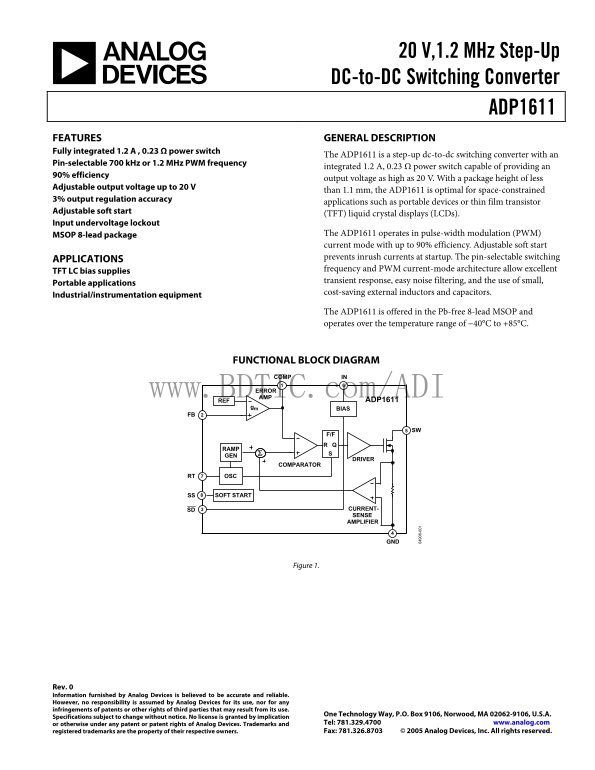
FUNCTIONAL BLOCK DIAGRAM

COMP IN

www.BDTIC.com/ADI ERROR AMP

REF ADP1611

BIASgm

RAMP GEN

DRIVER

COMPARATOR

RT OSC

SOFT STARTSS

SD CURRENT- SENSE AMPLIFIER

Figure 1.

Rev. 0 Information furnished by Analog Devices is believed to be accurate and reliable. However, no responsibility is assumed by Analog Devices for its use, nor for any infringements of patents or other rights of third parties that may result from its use.

One Technology Way, P.O. Box 9106, Norwood, MA 02062-9106, U.S.A.

Specifications subject to change without notice. No license is granted by implication

or otherwise under any patent or patent rights of Analog Devices. Trademarks and Tel: 781.329.4700 www.analog.com registered trademarks are the property of their respective owners. Fax: 781.326.8703 © 2005 Analog Devices, Inc. All rights reserved.

Page Summary Contents For ADP1611 Analog Devices Data Sheet Manual

Page 1 20 V,1.2 MHz Step-Up DC-to-DC Switching Converter ADP1611 FEATURES GENERAL DESCRIPTION Fully integrated 1.2 A , 0.23 Ω power switch The ADP1611 is a step-up dc-to-dc switching converter with an Pin-se...
Page 2 ADP1611 TABLE OF CONTENTS Specifications..................................................................................... Choosing the Input and Output Capacitors Absolute Maximum Ratings............
Page 3 ADP1611 SPECIFICATIONS VIN = 3.3 V, TA = −40°C to +85°C, unless otherwise noted. All limits at temperature extremes are guaranteed by correlation and characterization using standard statistical qualit...
Page 4 ADP1611 ABSOLUTE MAXIMUM RATINGS Table 2. Stresses above those listed under Absolute Maximum Ratings may cause permanent damage to the device. This is a stress Parameter Rating rating only; functional...
Page 5 ADP1611 PIN CONFIGURATION AND FUNCTION DESCRIPTIONS COMP SS8 FB ADP1611 RT7 TOP VIEW SD IN6 (Not to Scale) GND SW5 Figure 3. Pin Configuration Table 3. Pin Function Descriptions Pin No. Mnemonic Descr...
Page 6 EF FI IE EF FI IE EF FI IE ADP1611 TYPICAL PERFORMANCE CHARACTERISTICS VIN = 5V VIN = 3.3V FSW = 700k Hz VOUT = 10V FSW = 1.2MHz VOUT = 5V VOUT = 13V VOUT = 20V VOUT = 15V VOUT = 8.5V 6- 6- 6- LOAD CU...
Page 7 ADP1611 EG LA TI LT (V SW IT ES IS TA (m SC IL LA TO FR EQ EN (M z) FSW = 700k Hz RT = VIN VFB = 1.3V VIN = 5.5V RT = GND 0.35 0.6 VIN = 3.3V VIN = 2.5V VOUT = 10V SUPPLY VOLTAGE (V) AMBIENT TEMPERATU...
Page 8 SH TD ES LD (V SW IT EA EN (µ SU PP LY EN (m ADP1611 2.0 FSW = 1.23k Hz VFB = 1V 1.8 VIN = 5.5V VIN = 3.3V 0.8 VIN = 2.5V AMBIENT TEMPERATURE (°C) AMBIENT TEMPERATURE (°C) Figure 16. Supply Current vs...
Page 9 ADP1611 VIN = 5V CH1 = IL 2A/DIV VIN = 5V VOUT = 20V CH2 = VOUT 10V/DIV VOUT = 20V COUT = 10µF CH3 = SD 1V/DIV IOUT = 200m A CH1 = ILOAD 200m A/DIV L = 10µH CH4 = COMP 2V/DIV CSS = 0F CH2 = VOUT 200m ...
Page 10 ADP1611 THEORY OF OPERATION The ADP1611 current-mode step-up switching converter ON/OFF CONTROL converts a 2.5 V to 5.5 V input voltage up to an output voltage The SD input turns the ADP1611 regulator...
Page 11 ADP1611 Table 4. Inductor Manufacturers Vendor Part L (µH) Max DC Current Max DCR (mΩ) Height (mm) Sumida CMD4D11-2R2MC 2.2 0.95 116 1.2 847-956-0666 CMD4D11-4R7MC 4.7 0.75 216 1.2 www.sumida.com CDRH...
Page 12 ADP1611 The regulator loop gain is DIODE SELECTION The output rectifier conducts the inductor current to the output VA FB IN ×××××= ZGZG (12) capacitor and load while the switch is off. For high effic...
Page 13 ADP1611 SOFT-START CAPACITOR For low ESR output capacitance, such as with a ceramic capaci- tor, C2 is optional. For optimal transient performance, the The voltage at SS ramps up slowly by charging th...
Page 14 ADP1611 APPLICATION CIRCUITS TFT LCD BIAS SUPPLY The circuit in Figure 27 shows the ADP1611 in a step-up Figure 29 shows a power supply circuit for TFT LCD module configuration. The ADP1611 is used he...
Page 15 ADP1611 SEPIC POWER SUPPLY The circuit in Figure 30 shows the ADP1611 in a single-ended L1 primary inductance converter (SEPIC) topology. This topology 4.7µH is useful for an unregulated input voltage...
Page 16 ADP1611 LAYOUT PROCEDURE To achieve high efficiency, good regulation, and stability, a well- • Keep high current traces as short and as wide as possible. designed printed circuit board layout is requi...
Page 17 ADP1611 Figure 32. Sample Application Board (Top Layer) www.BDTIC.com/ADI Figure 33. Sample Application Board (Silkscreen Layer) Rev. 0 | Page 17 of 20
Page 18 ADP1611 OUTLINE DIMENSIONS 3.00 BSC 3.00 4.90 BSC BSC PIN 1 0.65 BSC 0.15 1.10 MAX COPLANARITY SEATING 0.10 PLANE COMPLIANT TO JEDEC STANDARDS MO-187AA Figure 34. 8-Lead Mini Small Outline Package [MS...
Page 19 ADP1611 NOTES www.BDTIC.com/ADI Rev. 0 | Page 19 of 20
Page 20 ADP1611 NOTES www.BDTIC.com/ADI © 2005 Analog Devices, Inc. All rights reserved. Trademarks and registered trademarks are the property of their respective owners. D04906–0–2/05(0) Rev. 0 | Page 20 of ...

Manual Details

Brand Analog Devices
Pages 20
File Size 645.51 KB
Published June 05, 2026
52 views

Enter the captcha to get the download link:

captcha

Frequently Asked Questions

What is the maximum output voltage this device can supply?

It can provide an adjustable output voltage up to 20 V.

Does the converter prevent excessive current at startup?

Yes, the device features adjustable soft start capability to prevent inrush currents.

What are key considerations for PCB layout?

Keep high current traces short and wide; place feedback resistors as close to FB as possible.

What is the expected overall regulation accuracy?

The overall regulation accuracy is specified at ±3%.