AD8306 Analog Devices Data Sheet Manual
Summary
This high-precision log-limiting IF amplifier is engineered for accurate signal strength measurement across a 100 dB dynamic range, providing ideal decibel readings and RSSI functionality. Operating efficiently from 5 MHz to 400 MHz, it delivers stable power monitoring regardless of temperature or single supply variations. The technical manual covers its full operation, including functional block diagrams and detailed specifications. It is essential for designers building specialized receivers, advanced radar/sonar systems, network analyzers, and RF measurement instruments.
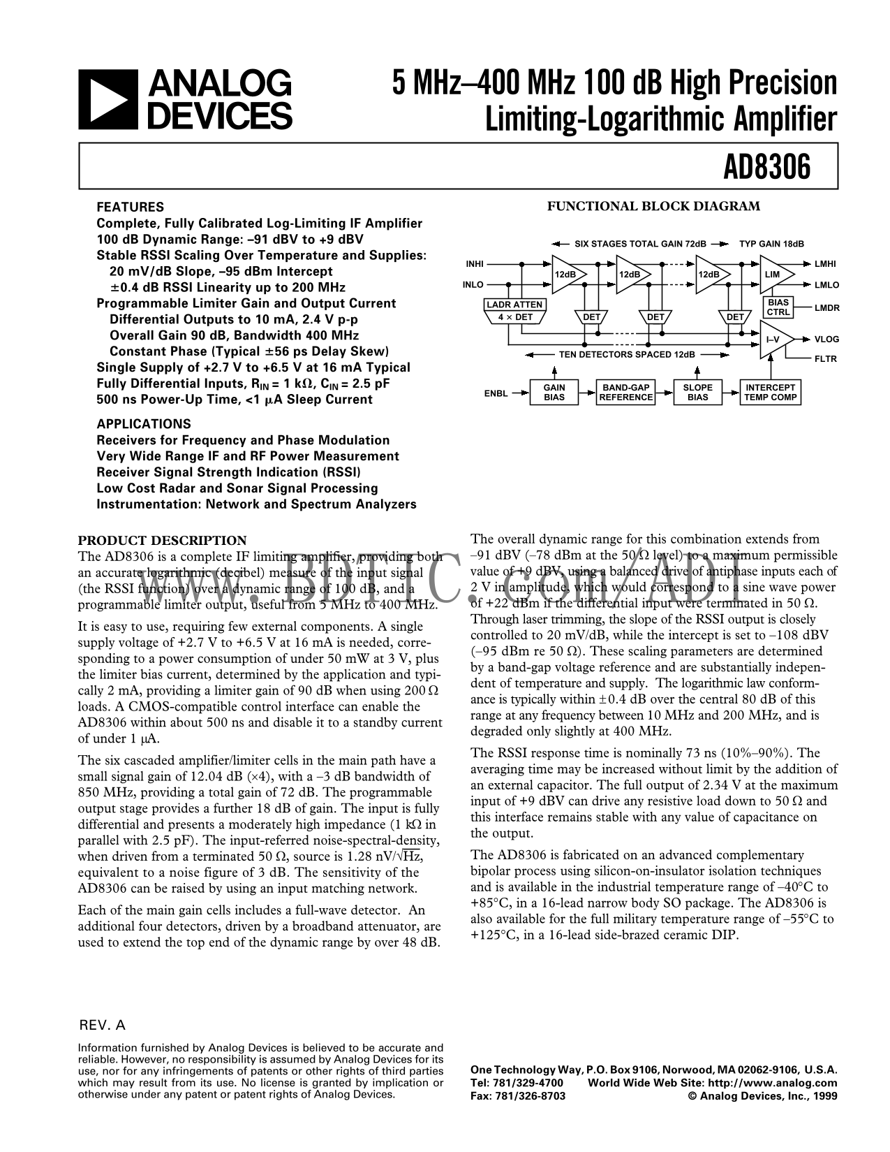
Page 1 Text Content
5 MHz–400 MHz 100 d B High Precision Limiting-Logarithmic Amplifier
AD8306
FUNCTIONAL BLOCK DIAGRAMFEATURES
Complete, Fully Calibrated Log-Limiting IF Amplifier 100 d B Dynamic Range: –91 d BV to +9 d BV
SIX STAGES TOTAL GAIN 72d B TYP GAIN 18d B
Stable RSSI Scaling Over Temperature and Supplies:
INHI LMHI
20 m V/d B Slope, –95 d Bm Intercept 12d B 12d B 12d B LIM
INLO LMLO
60.4 d B RSSI Linearity up to 200 MHz
Programmable Limiter Gain and Output Current LADR ATTEN BIAS
DET DET4 3 DET DET
Differential Outputs to 10 m A, 2.4 V p-p Overall Gain 90 d B, Bandwidth 400 MHz I–V VLOG Constant Phase (Typical 656 ps Delay Skew) TEN DETECTORS SPACED 12d B
Single Supply of +2.7 V to +6.5 V at 16 m A Typical Fully Differential Inputs, RIN = 1 k V, CIN = 2.5 p F GAIN BAND-GAP SLOPE INTERCEPT
BIAS REFERENCEENBL BIAS TEMP COMP
500 ns Power-Up Time, <1 m A Sleep Current
APPLICATIONS Receivers for Frequency and Phase Modulation Very Wide Range IF and RF Power Measurement Receiver Signal Strength Indication (RSSI) Low Cost Radar and Sonar Signal Processing Instrumentation: Network and Spectrum Analyzers
PRODUCT DESCRIPTION The overall dynamic range for this combination extends from The AD8306 is a complete IF limiting amplifier, providing both –91 d BV (–78 d Bm at the 50 Ω level) to a maximum permissible an accurate logarithmic (decibel) measure of the input signal value of +9 d BV, using a balanced drive of antiphase inputs each of (the RSSI function) over a dynamic range of 100 d B, and a 2 V in amplitude, which would correspond to a sine wave power
www.BDTIC.com/ADI
programmable limiter output, useful from 5 MHz to 400 MHz. of +22 d Bm if the differential input were terminated in 50 Ω. Through laser trimming, the slope of the RSSI output is closely
It is easy to use, requiring few external components. A single
controlled to 20 m V/d B, while the intercept is set to –108 d BV
supply voltage of +2.7 V to +6.5 V at 16 m A is needed, corre-
(–95 d Bm re 50 Ω). These scaling parameters are determined
sponding to a power consumption of under 50 m W at 3 V, plus
by a band-gap voltage reference and are substantially indepen-
the limiter bias current, determined by the application and typi-
dent of temperature and supply. The logarithmic law conform-
cally 2 m A, providing a limiter gain of 90 d B when using 200
ance is typically within ±0.4 d B over the central 80 d B of this
loads. A CMOS-compatible control interface can enable the
range at any frequency between 10 MHz and 200 MHz, and is
AD8306 within about 500 ns and disable it to a standby current
degraded only slightly at 400 MHz.
of under 1 µA.
The RSSI response time is nominally 73 ns (10%–90%). The
The six cascaded amplifier/limiter cells in the main path have a
averaging time may be increased without limit by the addition of
small signal gain of 12.04 d B (×4), with a –3 d B bandwidth of
an external capacitor. The full output of 2.34 V at the maximum
850 MHz, providing a total gain of 72 d B. The programmable
input of +9 d BV can drive any resistive load down to 50 Ω and
output stage provides a further 18 d B of gain. The input is fully
this interface remains stable with any value of capacitance on
differential and presents a moderately high impedance (1 kΩ in
the output.
parallel with 2.5 p F). The input-referred noise-spectral-density,
when driven from a terminated 50 Ω, source is 1.28 n V/√Hz, The AD8306 is fabricated on an advanced complementary equivalent to a noise figure of 3 d B. The sensitivity of the bipolar process using silicon-on-insulator isolation techniques AD8306 can be raised by using an input matching network. and is available in the industrial temperature range of –40°C to +85°C, in a 16-lead narrow body SO package. The AD8306 is
Each of the main gain cells includes a full-wave detector. An
also available for the full military temperature range of –55°C to
additional four detectors, driven by a broadband attenuator, are
+125°C, in a 16-lead side-brazed ceramic DIP.
used to extend the top end of the dynamic range by over 48 d B.
REV. A Information furnished by Analog Devices is believed to be accurate and reliable. However, no responsibility is assumed by Analog Devices for its
use, nor for any infringements of patents or other rights of third parties One Technology Way, P.O. Box 9106, Norwood, MA 02062-9106, U.S.A.
which may result from its use. No license is granted by implication or Tel: 781/329-4700 World Wide Web Site: http://www.analog.com otherwise under any patent or patent rights of Analog Devices. Fax: 781/326-8703 © Analog Devices, Inc., 1999
Page Summary Contents For AD8306 Analog Devices Data Sheet Manual
Manual Details
| Brand | Analog Devices |
|---|---|
| Pages | 16 |
| File Size | 390.20 KB |
| Published | July 16, 2026 |
Enter the captcha to get the download link:

Frequently Asked Questions
What is the overall dynamic range of the AD8306?
The overall dynamic range extends from -91 dBV to +9 dBV, with a total capacity of 100 dB.
How can I adjust the RSSI output slope and bandwidth?
Slope is adjusted by adding a resistive divider (R3/R4). Bandwidth adjustment involves using an external capacitor C7 in the VLOG output line to lower the frequency response.
What are the recommended supply voltage parameters?
It operates with a single supply of +2.7 V to +6.5 V at 16 mA, consuming under 50 mW at 3 V.
Does this component offer different temperature ratings?
Yes, it is available in industrial range (-40°C to +85°C), and also supports a military range (-55°C to +125°C).