# A B C D E F G H I J K L M N O P Q R S T U V W X Y Z

AD7942 Analog Devices Data Sheet Manual

Summary

The AD7942 is a high-performance, 14-bit SAR ADC featuring up to 250 kSPS throughput and exceptional power efficiency for demanding applications. This comprehensive guide details the product's operation, covering crucial aspects like single-supply compatibility, pseudo-differential inputs, and versatile daisy-chaining via SPI. It is designed for engineers developing sophisticated data acquisition systems in medical instrumentation, industrial process control, and advanced scientific equipment requiring high accuracy and low power consumption.
📄 Preview 📖 Table of Contents Contents PAGE OF 24

Page 1 Text Content

14-Bit, 250 k SPS Pul SAR,

Pseudo Differential ADC in MSOP/QFN

AD7942 FEATURES APPLICATION DIAGRAM

0.5V TO 5V 2.5V TO 5V

14-bit resolution with no missing codes Throughput: 250 k SPS INL: ±0.4 LSB typical, ±1 LSB maximum (±0.0061% of FSR)

SINAD: 85 d B @ 20 k Hz REF VDD VIO 1.8V TO VDD

0V TO VREF

THD: −100 d B @ 20 k Hz IN+

AD7942 SCK 3- OR 4-WIRE INTERFACE

Pseudo differential analog input range IN–

SDO (SPI, DAISY CHAIN, CS)

0 V to VREF with VREF up to VDD GND CNV No pipeline delay Single-supply 2.3 V to 5.5 V operation with 1.8 V/2.5 V/3 V/5 V logic interface

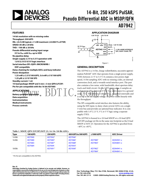
Figure 1.

Serial interface SPI-/QSPI-/MICROWIRE-/ DSP-compatible GENERAL DESCRIPTION Daisy-chaining for multiple ADCs and busy indicator

The AD7942 is a 14-bit, charge redistribution, successive approxi-

Power dissipation

mation Pul SAR® ADC that operates from a single power supply,

1.25 m W @ 2.5 V/100 k SPS, 3.6 m W @ 5 V/100 k SPS

VDD, between 2.3 V to 5.5 V. It contains a low power, high

1.25 μW @ 2.5 V/100 SPS

speed, 14-bit sampling ADC with no missing codes, an internal

Standby current: 1 n A

conversion clock, and a versatile serial interface port. The part

10-lead package: MSOP and 3 mm × 3 mm QFN (LFCSP)

also contains a low noise, wide bandwidth, short aperture delay

Pin-for-pin compatible with the 16-bit AD7685

track-and-hold circuit. On the CNV rising edge, it samples an

APPLICATIONS analog input, IN+, between 0 V to VREF with respect to a ground

sense, IN−. The reference voltage, VREF, is applied externally and

Battery-powered equipment ww.BDTIC.c m/ADI

is set up to be the supply voltage. Its power scales linearly with

Data acquisition

the throughput.

Instrumentation Medical instruments The SPI-compatible serial interface also features the ability, Process controls using the SDI input, to daisy-chain several ADCs on a single

3-wire bus and provides an optional busy indicator. It is com- patible with 1.8 V, 2.5 V, 3 V, or 5 V logic using a separate supply (VIO). The AD7942 is housed in a 10-lead MSOP or a 10-lead QFN (LFCSP) package yet fits in the same size footprint as the 8-lead MSOP or SOT-23. Operation for the AD7942 is specified from −40°C to +85°C.

Table 1. MSOP, QFN (LFCSP)/SOT-23, 14-/16-/18-Bit ADCs

Type 100 k SPS 250 k SPS 400 k SPS to 500 k SPS ≥1000 k SPS ADC Driver 14-Bit AD7940 AD79421 AD79461 16-Bit AD7680 AD76861 AD79801 AD76851 ADA4941-x AD7683 AD76871 AD76881 AD79831 ADA4841-x AD7684 AD7694 AD76931 18-Bit AD76911 AD76901 AD79821 ADA4941-x AD79841 ADA4841-x

1 Pin-for-pin compatible to the AD7942.

Rev. B Information furnished by Analog Devices is believed to be accurate and reliable. However, no responsibility is assumed by Analog Devices for its use, nor for any infringements of patents or other

One Technology Way, P.O. Box 9106, Norwood, MA 02062-9106, U.S.A.

rights of third parties that may result from its use. Specifications subject to change without notice. No

license is granted by implication or otherwise under any patent or patent rights of Analog Devices. Tel: 781.329.4700 www.analog.com Trademarks and registered trademarks are the property of their respective owners. Fax: 781.461.3113 ©2005–2008 Analog Devices, Inc. All rights reserved.

Page Summary Contents For AD7942 Analog Devices Data Sheet Manual

Page 1 14-Bit, 250 k SPS Pul SAR, Pseudo Differential ADC in MSOP/QFN AD7942 FEATURES APPLICATION DIAGRAM 0.5V TO 5V 2.5V TO 5V 14-bit resolution with no missing codes Throughput: 250 k SPS INL: ±0.4 LSB typ...
Page 2 AD7942 TABLE OF CONTENTS Features .............................................................................................. 1 Terminology ............................................................
Page 3 AD7942 SPECIFICATIONS VDD = 2.3 V to 5.5 V, VIO = 2.3 V to VDD, VREF = VDD, TA = –40°C to +85°C, unless otherwise noted. Table 2. Parameter Conditions Min Typ Max Unit RESOLUTION 14 Bits ANALOG INPUT ...
Page 4 AD7942 Parameter Conditions Min Typ Max Unit DIGITAL OUTPUTS Data Format Serial 14 bits straight binary Pipeline Delay Conversion results available immediately after completed conversion VOL ISINK = +...
Page 5 AD7942 TIMING SPECIFICATIONS VDD = 4.5 V to 5.5 V1, VIO = 2.3 V to 5.5 V or VDD + 0.3 V, whichever is the lowest, unless otherwise stated, TA = −40°C to +85°C. Table 3. Parameter Symbol Min Typ Max Un...
Page 6 AD7942 VDD = 2.3 V to 4.5 V1, VIO = 2.3 V to 4.5 V or VDD + 0.3 V, whichever is the lowest, unless otherwise stated, TA = −40°C to +85°C. Table 4. Parameter Symbol Min Typ Max Unit Conversion Time: CN...
Page 7 AD7942 ABSOLUTE MAXIMUM RATINGS Table 5. Parameter Rating Stresses above those listed under Absolute Maximum Ratings Analog Inputs may cause permanent damage to the device. This is a stress IN+1, IN−1...
Page 8 AD7942 PIN CONFIGURATION AND FUNCTION DESCRIPTIONS REF VIO10 VDD SDI9 IN+ AD7942 SCK8 IN– SDO7 GND CNV6 NOTES 1. PADDLE CONNECTED TO GND. THIS CONNECTION IS NOT REQUIRED TO MEET THE ELECTRICAL PERFORM...
Page 9 AD7942 TS IN (L SB PL IT (d f F ul l S ca le TYPICAL PERFORMANCE CHARACTERISTICS 1.00 1.00 POSITIVE INL = +0.22LSB POSITIVE DNL = +0.24LSB NEGATIVE INL = –0.34LSB NEGATIVE DNL = –0.12LSB CODE CODE Fig...
Page 10 SN , S IN (d SN (d AD7942 SI (d VREF = 2.5V, –1d B SINAD –95 14.0 VREF = 5V, –1d B ENOB –105 REFERENCE VOLTAGE (V) FREQUENCY (k Hz) Figure 11. SNR, SINAD, and ENOB vs. Reference Voltage 7- Figure 14. ...
Page 11 AD7942 PE TI EN TS (µ PO ER -D EN TS (n OFFSET ERROR –2 GAIN ERROR VDD + VIO TEMPERATURE (°C) TEMPERATURE (°C) Figure 17. Power-Down Currents vs. Temperature Figure 19. Offset Error and Gain Error vs....
Page 12 AD7942 TERMINOLOGY Effective Number of Bits (ENOB) Linearity Error or Integral Nonlinearity Error (INL) ENOB is a measurement of the resolution with a sine wave Linearity error refers to the deviation...
Page 13 AD7942 THEORY OF OPERATION IN+ SWITCHES CONTROL LSB SW+MSB CONTROL LOGIC OUTPUT CODE LSB SW–MSB Figure 21. ADC Simplified Schematic During the acquisition phase, terminals of the array tied to the CIR...
Page 14 (S TR IG IN RY AD7942 (NOTE 1) REF 5V 10µF 100n F (NOTE 2) 1.8V TO VDD REF VDD VIO IN+ SDI 0V TO VREF 2.7n F(NOTE 3) AD7942 3- OR 4-WIRE INTERFACE (NOTE 5) IN– CNV (NOTE 4) NOTE 1: SEE THE VOLTAGE REF...
Page 15 AD7942 TH (d (d Driver Amplifier Choice VDD = 5V Although the AD7942 is easy to drive, the driver amplifier needs to meet the following requirements: • The noise generated by the driver amplifier need...
Page 16 PE AT IN EN (µ PS (d AD7942 Power Supply • A reference voltage with enough current output capability, such as the ADR43x, or The AD7942 is specified over a wide operating range from 2.3 V to 5.5 V. It...
Page 17 AD7942 minimum conversion time and held high until the maximum CS Mode 3-Wire Without Busy Indicator conversion time to avoid generating the busy signal indicator. This mode is most often used when a ...
Page 18 AD7942 CS Mode 3-Wire with Busy Indicator low until the maximum conversion time to guarantee the generation of the busy signal indicator. When the conversion This mode is most often used when a single...
Page 19 AD7942 CS Mode 4-Wire Without Busy Indicator enters the acquisition phase and powers down. Each ADC result can be read by bringing its SDI input low, which consequently This mode is most often used wh...
Page 20 AD7942 CS Mode 4-Wire with Busy Indicator but SDI must be returned low before the minimum conversion time elapses and held low until the maximum conversion time This mode is most often used when a sin...
Page 21 AD7942 Chain Mode Without Busy Indicator and powers down. The remaining data bits stored in the inter- nal shift register are then clocked by subsequent SCK falling This mode can be used to daisy-chai...
Page 22 AD7942 Chain Mode with Busy Indicator can be used as a busy indicator to trigger the data readback controlled by the digital host. The AD7942 then enters the This mode can also be used to daisy-chain ...
Page 23 AD7942 APPLICATION HINTS LAYOUT Design the PCB that houses the AD7942 so that the analog and digital sections are separated and confined to certain areas of the board. The pinout of the AD7942, with a...
Page 24 AD7942 OUTLINE DIMENSIONS PIN 1 0.50 BSC 0.95 0.85 1.10 MAX 0.75 0.33 SEATING 0.23 0.05 0.17 PLANE 0.40 COPLANARITY 0.10 COMPLIANT TO JEDEC STANDARDS MO-187-BA Figure 44. 10-Lead Mini Small Outline Pa...

Manual Details

Brand Analog Devices
Pages 24
File Size 534.02 KB
Published June 15, 2026
2 views

Enter the captcha to get the download link:

captcha

Frequently Asked Questions

How can I connect multiple ADCs using this device?

The SDI input allows you to daisy-chain several ADCs on a single 3-wire bus.

What logic voltage levels are supported for the serial interface?

It is compatible with 1.8V, 2.5V, 3V, or 5V logic using a separate VIO supply.

How does the power consumption relate to data acquisition speed?

The device's power scales linearly with the throughput.

What are the specified operating temperature limits for the AD7942?

Operation is specified from -40°C to +85°C.