# A B C D E F G H I J K L M N O P Q R S T U V W X Y Z

AD7760 Analog Devices Data Sheet Manual

Summary

The AD7760 is a high-performance, 24-bit Sigma-Delta Analog-to-Digital Converter (ADC) offering robust features like an integrated buffer and programmable decimation filters. It delivers exceptional signal integrity with up to 100 dB dynamic range at 2.5 MSPS. This manual provides comprehensive technical details, covering the functional architecture, configuration registers, and operating modes necessary for integration. It is perfectly suited for engineers developing advanced data acquisition systems, vibration analyzers, or precision instrumentation that requires high Signal-to-Noise Ratio (SNR) in demanding environments.
📄 Preview 📖 Table of Contents Contents PAGE OF 36

Page 1 Text Content

2.5 MSPS, 24-Bit, 100 d B

Sigma-Delta ADC with On-Chip Buffer

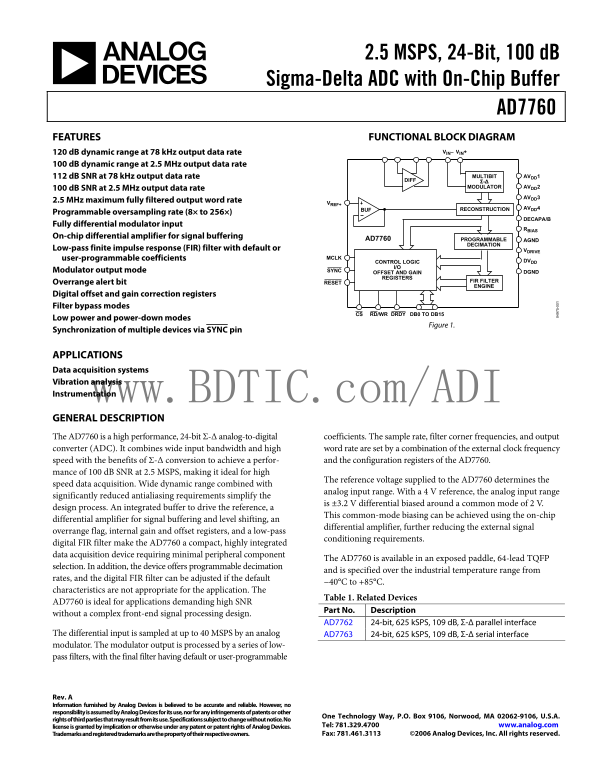
AD7760 FEATURES FUNCTIONAL BLOCK DIAGRAM

120 d B dynamic range at 78 k Hz output data rate VIN+VIN–

100 d B dynamic range at 2.5 MHz output data rate

112 d B SNR at 78 k Hz output data rate MULTIBIT AVDD1

DIFF Σ-Δ

100 d B SNR at 2.5 MHz output data rate MODULATOR AVDD2 AVDD3

2.5 MHz maximum fully filtered output word rate

VREF+

BUF RECONSTRUCTION AVDD4

Programmable oversampling rate (8× to 256×)

DECAPA/B

Fully differential modulator input

RBIAS

On-chip differential amplifier for signal buffering

AD7760 PROGRAMMABLE AGND

DECIMATION

Low-pass finite impulse response (FIR) filter with default or VDRIVE

user-programmable coefficients MCLK

CONTROL LOGIC DVDD

Modulator output mode SYNC OFFSET AND GAIN DGND

REGISTERS

Overrange alert bit RESET FIR FILTER ENGINE

Digital offset and gain correction registers Filter bypass modes

DRDYRD/WR DB0 TO DB15CS

Low power and power-down modes

Figure 1.

Synchronization of multiple devices via SYNC pin

APPLICATIONS Data acquisition systems Vibration analysis Instrumentation

www.BDTIC.com/ADI GENERAL DESCRIPTION The AD7760 is a high performance, 24-bit Σ-Δ analog-to-digital coefficients. The sample rate, filter corner frequencies, and output converter (ADC). It combines wide input bandwidth and high word rate are set by a combination of the external clock frequency

speed with the benefits of Σ-Δ conversion to achieve a perfor- and the configuration registers of the AD7760.

mance of 100 d B SNR at 2.5 MSPS, making it ideal for high

The reference voltage supplied to the AD7760 determines the

speed data acquisition. Wide dynamic range combined with

analog input range. With a 4 V reference, the analog input range

significantly reduced antialiasing requirements simplify the

is ±3.2 V differential biased around a common mode of 2 V.

design process. An integrated buffer to drive the reference, a

This common-mode biasing can be achieved using the on-chip

differential amplifier for signal buffering and level shifting, an

differential amplifier, further reducing the external signal

overrange flag, internal gain and offset registers, and a low-pass

conditioning requirements.

digital FIR filter make the AD7760 a compact, highly integrated data acquisition device requiring minimal peripheral component 5-

The AD7760 is available in an exposed paddle, 64-lead TQFP

selection. In addition, the device offers programmable decimation

and is specified over the industrial temperature range from

rates, and the digital FIR filter can be adjusted if the default

−40°C to +85°C.

characteristics are not appropriate for the application. The

Table 1. Related Devices

AD7760 is ideal for applications demanding high SNR

Part No. Description

without a complex front-end signal processing design.

AD7762 24-bit, 625 k SPS, 109 d B, Σ-Δ parallel interface

The differential input is sampled at up to 40 MSPS by an analog AD7763 24-bit, 625 k SPS, 109 d B, Σ-Δ serial interface modulator. The modulator output is processed by a series of low- pass filters, with the final filter having default or user-programmable

Rev. A Information furnished by Analog Devices is believed to be accurate and reliable. However, no responsibility is assumed by Analog Devices for its use, nor for any infringements of patents or other

One Technology Way, P.O. Box 9106, Norwood, MA 02062-9106, U.S.A.

rights of third parties that may result from its use. Specifications subject to change without notice. No

license is granted by implication or otherwise under any patent or patent rights of Analog Devices. Tel: 781.329.4700 www.analog.com Trademarks and registered trademarks are the property of their respective owners. Fax: 781.461.3113 ©2006 Analog Devices, Inc. All rights reserved.

Page Summary Contents For AD7760 Analog Devices Data Sheet Manual

Page 1 2.5 MSPS, 24-Bit, 100 d B Sigma-Delta ADC with On-Chip Buffer AD7760 FEATURES FUNCTIONAL BLOCK DIAGRAM 120 d B dynamic range at 78 k Hz output data rate VIN+VIN– 100 d B dynamic range at 2.5 MHz outpu...
Page 2 AD7760 TABLE OF CONTENTS Features Writing to the AD7760 Applications....................................................................................... Clocking the AD7760 Functional Block Diagram...
Page 3 AD7760 REVISION HISTORY 8/06—Rev. 0 to Rev. A Updated Package Option................................................... Universal Added MCLK Jitter Requirements Heading ..................................
Page 4 AD7760 SPECIFICATIONS AVDD1 = DVDD = VDRIVE = 2.5 V, AVDD2 = AVDD3 = AVDD4 = 5 V, VREF+ = 4.096 V, MCLK amplitude = 5 V, TA = 25°C, normal mode, using the on-chip amplifier with components as shown in...
Page 5 AD7760 Parameter Test Conditions/Comments Specification Unit ANALOG INPUT Differential Input Voltage VIN(+) – VIN(−), VREF = 2.5 V ±2 V p-p VIN(+) – VIN(−), VREF = 4.096 V ±3.25 V p-p Input Capacitanc...
Page 6 AD7760 TIMING SPECIFICATIONS AVDD1 = DVDD = VDRIVE = 2.5 V, AVDD2 = AVDD3 = AVDD4 = 5 V, TA = 25°C, normal mode, unless otherwise noted. Table 3. Parameter Limit at TMIN, TMAX Unit Description f MCLK ...
Page 7 AD7760 TIMING DIAGRAMS RD/WR D[0:15] DATA MSW LSW STATUS Figure 2. Filtered Output—Parallel Interface Timing Diagram RD/WR D[0:15] REGISTER ADDRESS REGISTER DATA Figure 3. AD7760 Register Write www.BD...
Page 8 AD7760 ABSOLUTE MAXIMUM RATINGS TA = 25°C, unless otherwise noted. Table 4. Stresses above those listed under Absolute Maximum Ratings Parameters Rating may cause permanent damage to the device. This ...
Page 9 AD7760 PIN CONFIGURATION AND FUNCTION DESCRIPTIONS 1DGND DB12 2MCLKGND DB13 3MCLK DB14 4AVDD2 DB15 5AGND2 VDRIVE 6AVDD1 DGND 7AGND1 DGND AD7760 8DECAPA VIEW DVDD (Not to Scale) 9REFGND CS 10VREF+ RD/W...
Page 10 AD7760 Pin No. Mnemonic Description 30 DECAPB Decoupling Pin. A 33 p F capacitor must be inserted between this pin and AGND3. 17 RBIAS Bias Current Setting Pin. A resistor must be inserted between thi...
Page 11 AD7760 TERMINOLOGY Signal-to-Noise Ratio (SNR) Integral Nonlinearity (INL) SNR is the ratio of the rms value of the actual input signal to the INL is the maximum deviation from a straight line passing...
Page 12 PL IT (d PL IT (d PL IT (d AD7760 TYPICAL PERFORMANCE CHARACTERISTICS AVDD1 = DVDD = VDRIVE = 2.5 V, AVDD2 = AVDD3 = AVDD4 = 5 V, VREF = 4.096 V, TA = 25°C, normal mode, unless otherwise noted. All FF...
Page 13 AD7760 PL IT (d PL IT (d PL IT (d FREQUENCY (k Hz) FREQUENCY (k Hz) Figure 11. Normal Mode FFT, 100 k Hz, −0.5 d B Input Tone, 8× Decimation Figure 14. Low Power FFT, 100 k Hz, −0.5 d B Input Tone, 8×...
Page 14 AD7760 PL IT (d PL IT (d PL IT (d FREQUENCY (k Hz) FREQUENCY (k Hz) Figure 17. Normal Mode FFT, 1 MHz, −6 d B Input Tone, 8× Decimation Figure 20. Low Power FFT, 1 MHz, −6 d B Input Tone, 8× Decimatio...
Page 15 AD7760 SN (d FS SN (d FS PL IT (d TONE A: 999.75k Hz TONE A: 999.75k Hz TONE B: 1.00025MHz TONE B: 1.00025MHz –20 –20 THIRD-ORDER THIRD-ORDER IMD: –89.15d B IMD: –87.67d B –40 –40 FREQUENCY (k Hz) FRE...
Page 16 IN EN EN AD7760 24-BIT CODE 24-BIT CODE Figure 29. Normal Mode, 24-Bit Histogram, 256× Decimation 5- Figure 32. Low Power, 24-Bit Histogram, 256× Decimation IN )0.0005 EN EN www.BDTIC.com/ADI 24-BIT C...
Page 17 AD7760 (L SB 24-BIT CODE ICLK FREQUENCY (MHz) Figure 35. 24-Bit DNL Figure 38. Decimate × 32, DIDD vs. ICLK Frequency (DVDD = 2.5 V) www.BDTIC.com/ADI ICLK FREQUENCY (MHz) ICLK FREQUENCY (MHz) Figure ...
Page 18 AD7760 THEORY OF OPERATION The AD7760 employs a Σ-Δ conversion technique to convert The third filter has a fixed decimation rate of 2×, is user the analog input into an equivalent digital word. The mo...
Page 19 AD7760 PL IT (d MODULATOR DATA OUTPUT MODE scaled to 15 bits. The transfer function in Figure 42 shows the Operating the AD7760 in modulator output mode enables the scaling involved for the 16 data bi...
Page 20 AD7760 MODULATOR DATA OUTPUT MODE INTERFACE output mode when operating with CDIV = 1 (that is, ICLK = The AD7760 can be configured in modulator data output mode MCLK). A DRDY pulse is generated for ea...
Page 21 AD7760 D[0:15] INVALID DATA MOD DATA MOD DATA MOD D... CS, RD/WR Figure 45. AD7760 Modulator Output Mode (CDIV = 0, n is odd) In the case where n is an odd number of MCLK cycles, the 5. Write to Contr...
Page 22 AD7760 AD7760 INTERFACE READING DATA If multiple synchronized AD7760 parts that share a properly distributed common MCLK signal exist in a system, these parts When the AD7760 is outputting data at a 5...
Page 23 AD7760 Figure 3 shows a write operation to the AD7760. The RD/WR WRITING TO THE AD7760 line is held high while the CS line is brought low for a minimum There are many features and parameters that the ...
Page 24 AD7760 CLOCKING THE AD7760 The AD7760 requires an external low jitter clock source. This MCLK JITTER REQUIREMENTS signal is applied to the MCLK pin, and the MCLKGND pin is The MCLK jitter requirements...
Page 25 AD7760 1.0 1.0 Figure 48. Maximum Slew Rate of Sine Wave with Amplitude of 2 V p-p Figure 49. Maximum Slew Rate of Sine Wave (with the Same Frequency as in Figure 48) with Amplitude of 1 V p-p www.BDT...
Page 26 AD7760 DRIVING THE AD7760 signal to sit on the optimum common mode of VREF/2, in this The AD7760 has an on-chip differential amplifier that operates case 2.048 V. The signal is also scaled to give the...
Page 27 AD7760 To obtain maximum performance from the AD7760, it is USING THE AD7760 advisable to drive the ADC with differential signals. Figure 53 The following is the recommended sequence for powering up s...
Page 28 AD7760 DECOUPLING AND LAYOUT RECOMMENDATIONS Due to the high performance nature of the AD7760, correct decoupling and layout techniques are required to obtain the performance as stated within this dat...
Page 29 AD7760 SUPPLY DECOUPLING BIAS RESISTOR SELECTION Every supply pin must be connected to the appropriate supply The AD7760 requires a resistor to be connected between the via a ferrite bead and decouple...
Page 30 AD7760 PROGRAMMABLE FIR FILTER As previously mentioned, the third FIR filter on the AD7760 To create a filter, note the following: is user programmable. The default coefficients that are loaded • The ...
Page 31 AD7760 DOWNLOADING A USER-DEFINED FILTER As previously mentioned, the filter coefficients are 27 bits in EXAMPLE FILTER DOWNLOAD length—one sign and 26 magnitude bits. Because the AD7760 The following...
Page 32 AD7760 Table 13 shows the hexadecimal values (in sign-and-magnitude Table 14 lists the 16-bit words the user would write to the format) that are downloaded to the AD7760 to realize this filter. AD7760...
Page 33 AD7760 AD7760 REGISTERS The AD7760 has a number of user-programmable registers. The control registers are used to set the decimation rate, the filter configuration, the clock divider, and so on. There...
Page 34 AD7760 STATUS REGISTER (READ ONLY) MSB LSB D15 D14 D13 D12 D11 D10 D9 D8 D7 D6 D5 D4 D3 D2 D1 D0 PART 1 PART 0 DIE 2 DIE 1 DIE 0 LPWR OVR DL_OK FILTOK UFILT BYP F3 BYP F1 DEC2 DEC1 DEC0 Table 17. Bit ...
Page 35 AD7760 OUTLINE DIMENSIONS 12.20 12.00 SQ MAX0.75 PIN 1 10.20 10.00 SQ TOP VIEW EXPOSED 6.00 (PINS DOWN) 9.80 PAD BSC SQ 1.05 0° MIN 1.00 BOTTOM VIEW 0.95 (PINS UP) SEATING 0.05 PLANE 0.08 MAX VIEW A C...
Page 36 AD7760 NOTES www.BDTIC.com/ADI ©2006 Analog Devices, Inc. All rights reserved. Trademarks and registered trademarks are the property of their respective owners. D04975-0-8/06(A) Rev. A | Page 36 of 36

Manual Details

Brand Analog Devices
Pages 36
File Size 888.98 KB
Published June 16, 2026
1 views

Enter the captcha to get the download link:

captcha

Frequently Asked Questions

What is the dynamic range when using a 4V reference voltage?

It provides up to 120 dB dynamic range at 78 kHz and 112 dB SNR at 78 kHz.

How does the device handle overrange conditions?

The overrange alert bit is set immediately if the analog input exceeds 100% of V_REF, which sets the DVALID bit to zero.

What is the recommended operating temperature range for this model?

The AD7760BSVZ operates from -40°C to +85°C.

Can the device be used in mixed signal acquisition systems?

Yes, it is ideal for data acquisition systems, vibration analysis, and instrumentation demanding high SNR.