# A B C D E F G H I J K L M N O P Q R S T U V W X Y Z

AD7327 Analog Devices Data Sheet Manual

Summary

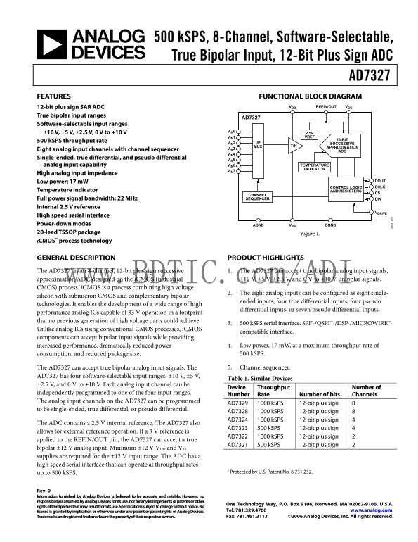
The AD7327 is an advanced 8-channel, 12-bit successive approximation Analog-to-Digital Converter (ADC) built for high-precision data acquisition. Engineered to robustly handle true bipolar analog input signals, it offers software-selectable ranges up to ±10V with low power consumption of only 17 mW. With a speed of 500 kSPS, this module is essential for engineers building complex measurement and monitoring systems requiring accurate signal capture in challenging environments. The provided manual details the device's setup, functional block diagram, registers, and optimized operational guidelines.
📄 Preview 📖 Table of Contents Contents PAGE OF 36

Page 1 Text Content

500 k SPS, 8-Channel, Software-Selectable, True Bipolar Input, 12-Bit Plus Sign ADC

AD7327 FEATURES FUNCTIONAL BLOCK DIAGRAM

12-bit plus sign SAR ADC VDD REFIN/OUT VCC

True bipolar input ranges

AD7327

Software-selectable input ranges

±10 V, ±5 V, ±2.5 V, 0 V to +10 V 2.5V

VIN1 VREF

13-BIT

500 k SPS throughput rate

VIN2 I/P SUCCESSIVE

MUX T/H

VIN3 APPROXIMATION

Eight analog input channels with channel sequencer

Single-ended, true differential, and pseudo differential

analog input capability VIN6 TEMPERATURE INDICATOR

High analog input impedance

Low power: 17 m W DOUT CONTROL LOGIC SCLK

Temperature indicator AND REGISTERS

CHANNEL Full power signal bandwidth: 22 MHz SEQUENCER DIN

Internal 2.5 V reference

VDRIVE

High speed serial interface Power-down modes AGND VSS DGND 20-lead TSSOP package

Figure 1.

i CMOS™ process technology

GENERAL DESCRIPTION PRODUCT HIGHLIGHTS The AD73271 is an 8-channel, 12-bit plus sign successive 1. The AD7327 can accept true bipolar analog input signals,

approximation ADC designed on the i CMOS (industrial www.BDTIC.com/ADI ±10 V, ±5 V, ±2.5 V, and 0 V to +10 V unipolar signals.

CMOS) process. i CMOS is a process combining high voltage

2. The eight analog inputs can be configured as eight single-

silicon with submicron CMOS and complementary bipolar

ended inputs, four true differential inputs, four pseudo

technologies. It enables the development of a wide range of high

differential inputs, or seven pseudo differential inputs.

performance analog ICs capable of 33 V operation in a footprint that no previous generation of high voltage parts could achieve.

3. 500 k SPS serial interface. SPI®-/QSPI™-/DSP-/MICROWIRE™-

Unlike analog ICs using conventional CMOS processes, i CMOS

compatible interface.

components can accept bipolar input signals while providing

increased performance, dramatically reduced power 4. Low power, 17 m W, at a maximum throughput rate of consumption, and reduced package size. 500 k SPS.

The AD7327 can accept true bipolar analog input signals. The 5. Channel sequencer.

AD7327 has four software-selectable input ranges, ±10 V, ±5 V,

Table 1. Similar Devices

±2.5 V, and 0 V to +10 V. Each analog input channel can be

Device Throughput Number of

independently programmed to one of the four input ranges. 1-

Number Rate Number of bits Channels

The analog input channels on the AD7327 can be programmed

AD7329 1000 k SPS 12-bit plus sign 8

to be single-ended, true differential, or pseudo differential.

AD7328 1000 k SPS 12-bit plus sign 8 AD7324 1000 k SPS 12-bit plus sign 4

The ADC contains a 2.5 V internal reference. The AD7327 also

AD7323 500 k SPS 12-bit plus sign 4

allows for external reference operation. If a 3 V reference is

AD7322 1000 k SPS 12-bit plus sign 2

applied to the REFIN/OUT pin, the AD7327 can accept a true

AD7321 500 k SPS 12-bit plus sign 2

bipolar ±12 V analog input. Minimum ±12 V VDD and VSS supplies are required for the ±12 V input range. The ADC has a high speed serial interface that can operate at throughput rates

1 Protected by U.S. Patent No. 6,731,232.

up to 500 k SPS.

Rev. 0 Information furnished by Analog Devices is believed to be accurate and reliable. However, no responsibility is assumed by Analog Devices for its use, nor for any infringements of patents or other

One Technology Way, P.O. Box 9106, Norwood, MA 02062-9106, U.S.A.

rights of third parties that may result from its use. Specifications subject to change without notice. No

license is granted by implication or otherwise under any patent or patent rights of Analog Devices. Tel: 781.329.4700 www.analog.com Trademarks and registered trademarks are the property of their respective owners. Fax: 781.461.3113 ©2006 Analog Devices, Inc. All rights reserved.

Page Summary Contents For AD7327 Analog Devices Data Sheet Manual

Page 1 500 k SPS, 8-Channel, Software-Selectable, True Bipolar Input, 12-Bit Plus Sign ADC AD7327 FEATURES FUNCTIONAL BLOCK DIAGRAM 12-bit plus sign SAR ADC VDD REFIN/OUT VCC True bipolar input ranges AD7327...
Page 2 AD7327 TABLE OF CONTENTS Features Control Register Functional Block Diagram Sequence Register....................................................................... General Description Range Registers...
Page 3 AD7327 SPECIFICATIONS VDD = 12 V to 16.5 V, VSS = −12 V to −16.5 V, VCC = 2.7 V to 5.25 V, VDRIVE = 2.7 V to 5.25 V, VREF = 2.5 V to 3.0 V internal/external, f SCLK = 10 MHz, f S = 500 k SPS, TA = TMA...
Page 4 AD7327 B Version Parameter1 Min Typ Max Unit Test Conditions/Comments DC ACCURACY4 Resolution 13 Bits No Missing Codes 12-bit Bits Differential mode plus sign 11-bit Bits Single-ended/pseudo different...
Page 5 AD7327 B Version Parameter1 Min Typ Max Unit Test Conditions/Comments ANALOG INPUT Input Voltage Ranges Reference = 2.5 V; see Table 6 (Programmed via Range ±10 V VDD = 10 V min, VSS = −10 V min, VCC ...
Page 6 AD7327 B Version Parameter1 Min Typ Max Unit Test Conditions/Comments POWER REQUIREMENTS Digital inputs = 0 V or VDRIVE VDD 12 16.5 V See Table 6 VSS −12 −16.5 V See Table 6 VCC 2.7 5.25 V See Table 6...
Page 7 AD7327 TIMING SPECIFICATIONS VDD = 12 V to 16.5 V, VSS = −12 V to −16.5 V, VCC = 2.7 V to 5.25 V, VDRIVE = 2.7 V to 5.25 V, VREF = 2.5 V to 3.0 V internal/external, TA = TMAX to TMIN. Timing specifica...
Page 8 AD7327 ABSOLUTE MAXIMUM RATINGS TA = 25°C, unless otherwise noted Table 4. Stresses above those listed under Absolute Maximum Ratings Parameter Rating may cause permanent damage to the device. This is...
Page 9 AD7327 PIN CONFIGURATION AND FUNCTION DESCRIPTIONS CS SCLK DIN DGND DGND DOUT AD7327 AGND VIEW VDRIVE (Not to Scale) REFIN/OUT VCC VSS VDD VIN0 VIN2 VIN1 VIN3 VIN4 VIN6 VIN5 VIN7 Figure 3. TSSOP Pin C...
Page 10 ER (L SB SN (d SN (d AD7327 TYPICAL PERFORMANCE CHARACTERISTICS 1.0 VCC VDRIVE 5V INT/EXT 2.5V REFERENCE POINT FFT 0.8 TA 25°C ±10V RANGE VCC VDRIVE 5V –20 VDD, VSS ±15V +INL +0.55LSB VDD, VSS ±15V 0....
Page 11 AD7327 SI (d TH (d TH (d VCC VDRIVE 3V ±5V DIFF –55 VDD/VSS ±12V ±2.5V DIFF TA 25°C –60 f S 500k SPS ±5V SE INTERNAL REFERENCE 0V TO +10V SE ±2.5V SE ±10V SE ±10V DIFF ±10V DIFF 0V TO +10V DIFF ±10V S...
Page 12 ER (L SB (d ER EN ES AD7327 VCC 5V VDD/VSS ±12V 1.5 RANGE ±10V 10k SAMPLES 6k TA 25°C 1.0 INL 500k SPS ±5V RANGE VCC VDRIVE 5V INTERNAL REFERENCE SINGLE-ENDED MODE CODE ±VDD/VSS SUPPLY VOLTAGE (V) Fig...
Page 13 AD7327 TH (d –50 VCC VDRIVE 5V –55 VDD/VSS ±12V TA 25°C ±10V RANGE –60 INTERNAL REF RIN 4000Ω RANGE ±10V AND ±2.5V RIN 2000Ω –65 f S 500k SPS RIN 1000Ω SINGLE-ENDED MODE RIN 100Ω RIN 50Ω ±2.5V RANGE R...
Page 14 AD7327 TERMINOLOGY Differential Nonlinearity Negative Full-Scale Error This is the difference between the measured and the ideal 1 LSB This applies when using twos complement output coding and change ...
Page 15 AD7327 terms are usually at a frequency close to the input frequencies. Channel-to-Channel Isolation As a result, the second- and third-order terms are specified Channel-to-channel isolation is a meas...
Page 16 AD7327 THEORY OF OPERATION CIRCUIT INFORMATION The analog inputs can be configured as eight single-ended inputs, four true differential inputs, four pseudo differential The AD7327 is a fast, 8-channel...
Page 17 AD7327 CAPACITIVE The ideal transfer characteristic for the AD7327 when twos DAC complement coding is selected is shown in Figure 27. The ideal CS COMPARATOR transfer characteristic for the AD7327 whe...
Page 18 AD7327 The AD7327 enters track on the 14th SCLK rising edge. When C2R1 running the AD7327 at a throughput rate of 500 k SPS with a 10 MHz SCLK signal, the ADC has approximately 1.5 SCLK + t8 + t QUIET...
Page 19 AD7327 TYPICAL CONNECTION DIAGRAM Figure 32 shows a typical connection diagram for the AD7327. In this configuration, the AGND pin is connected to the analog VDD VCC ground plane of the system, and th...
Page 20 AD7327 (V (V (V ±5V RANGE ±5V RANGE ±5V RANGE RANGE RANGE ±2.5V RANGE ±10V RANGE –1 ±10V RANGE ±2.5V –2 RANGE –2 ±10V –3 RANGE ±5V RANGE VCC 3V –6 –5 VCC 5V ±2.5V VREF 3V VREF 2.5V RANGE ±16.5V VDD/VS...
Page 21 AD7327 ±5V RANGE ±5V RANGE The driver amplifier must be able to settle for a full-scale step to a 13-bit level, 0.0122%, in less than the specified acquisition RANGE ±10V RANGE time of the AD7327. An ...
Page 22 AD7327 REGISTERS The AD7327 has four programmable registers: the control register, sequence register, Range Register 1, and Range Register 2. These registers are write-only registers. ADDRESSING REGIS...
Page 23 AD7327 CONTROL REGISTER The control register is used to select the analog input channel, analog input configuration, reference, coding, and power mode. The control register is a write-only, 12-bit reg...
Page 24 AD7327 Table 11. Power Mode Selection PM1 PM0 Description 1 1 Full Shutdown Mode. In this mode, all internal circuitry on the AD7327 is powered down. Information in the control register is retained wh...
Page 25 AD7327 SEQUENCE REGISTER The sequence register on the AD7327 is an 8-bit, write-only register. Each of the eight analog input channels has one corresponding bit in the sequence register. To select an ...
Page 26 AD7327 SEQUENCER OPERATION POWER ON. DIN: WRITE TO RANGE REGISTER TO SELECT THE RANGE FOR EACH ANALOG INPUT CHANNEL. DOUT: CONVERSION RESULT FROM CHANNEL 0, ±10V RANGE, SINGLE-ENDED MODE. DIN: WRITE T...
Page 27 AD7327 If a change to one of the range registers is required during a Once the control register is configured to operate the AD7327 sequence, it is necessary to first stop the sequence by writing to i...
Page 28 AD7327 REFERENCE TEMPERATURE INDICATOR The AD7327 can operate with either the internal 2.5 V on-chip The AD7327 has an on-chip temperature indicator. The reference or an externally applied reference. ...
Page 29 AD7327 MODES OF OPERATION The AD7327 has several modes of operation that are designed The AD7327 remains fully powered up at the end of the to provide flexible power management options. These options ...
Page 30 AD7327 AUTOSHUTDOWN MODE As is the case with autoshutdown mode, the AD7327 enters standby on the 15th SCLK rising edge once the control register is (PM1 = 1, PM0 = 0) updated (see Figure 50). The part...
Page 31 AD7327 AV ER PO ER (m POWER VS. THROUGHPUT RATE The power consumption of the AD7327 varies with throughput VCC 5V VDD/VSS ±12V rate. The static power consumed by the AD7327 is very low, and TA 25°C si...
Page 32 AD7327 SERIAL INTERFACE Figure 53 shows the timing diagram for the serial interface of Data is clocked into the AD7327 on the SCLK falling edge. The the AD7327. The serial clock applied to the SCLK pi...
Page 33 AD7327 MICROPROCESSOR INTERFACING The serial interface on the AD7327 allows the part to be directly The frequency of the serial clock is set in the SCLKDIV register. connected to a range of different ...
Page 34 AD7327 APPLICATION HINTS LAYOUT AND GROUNDING To avoid radiating noise to other sections of the board, com- ponents, such as clocks, with fast switching signals should be The printed circuit board tha...
Page 35 AD7327 OUTLINE DIMENSIONS 4.50 4.40 4.30 6.40 BSC PIN 1 0.65 BSC 0.15 1.20 MAX 0°COPLANARITY 0.45 0.19 SEATING 0.10 PLANE COMPLIANT TO JEDEC STANDARDS MO-153-AC Figure 56. 20-Lead Thin Shrink Small Ou...
Page 36 AD7327 NOTES www.BDTIC.com/ADI ©2006 Analog Devices, Inc. All rights reserved. Trademarks and registered trademarks are the property of their respective owners. D05401–0–1/06(0) Rev. 0 | Page 36 of 36

Manual Details

Brand Analog Devices
Pages 36
File Size 668.98 KB
Published June 16, 2026
2 views

Enter the captcha to get the download link:

captcha

Frequently Asked Questions

What kinds of analog signals can the AD7327 accept?

It supports true bipolar inputs and can be configured for single-ended, true differential, or pseudo differential signals.

How many input ranges are supported by this ADC?

The AD7327 has four software-selectable input ranges: ±10 V, ±5 V, ±2.5 V, and 0 V to +10 V.

What is the maximum throughput rate of the device?

The unit can operate at a high speed serialization interface up to 500 kSPS.

Where should I place ground connections when using this chip?

Use an analog ground plane and allow digital lines to run under the AD7327 to prevent noise coupling.